This thread has been locked.

If you have a related question, please click the "Ask a related question" button in the top right corner. The newly created question will be automatically linked to this question.

CDCE62005: Chip's Output clock = 2.5 x [desired frequency]; Lock not active.

Part Number: CDCE62005

Dear,

I would like to ask a question regarding the CDCE62005 chip's operation.

I have used both TI GUI tool (CDCE62005 EVM Software 1.4.8) and my own calculation to yield the register table for configurating the chip. However, I failed to set my desired frequency at the outputs.

I have XTAL 25MHz at my only input clock source. And my register setting is as below:

REGISTERS
0 68840320
1 EB060321
2 EB260302
3 EB140303
4 68060314
5 10008B25
6 94BE03E6
7 FD91FDF7
8 80001A08

PORTS
0 FD
1 FF
2 DF
3 F9

INPUTS
PRI 25
SEC 0
AUX 25

EXTERNAL COMPONENTS
C4 1
R4 1
C5 1

My desired outputs are: CH1: disable; CH2: 100MHz (LVDS); CH3: 20MHz (LVDS); CH4: 41.67MHz (LVDS); CH5: Disable; AUX_OUT: 20MHz

(after writing these values to the chip; I read back all the values and they were all written correctly; also, I did trigger calibration bit after each registers writing to make sure the VCO got calibrated)

However, when I check the output with DSO; they are as follow:

CH1: disable; CH2: 250MHz; CH3: 50MHz;CH4:104MHz; CH5: disable; AUX_OUT: 50MHz.

Which means that all output got x2.5 multiplied compare to my desired values.

Also, the PLL LOCK pin is not active; when I change the detect window from 3.4ns to 28.6ns, the pin keeps toggling at all time.

Please let me know what is the cause of the issue and hopefully some hints to help resolve the problems.

Besides, I also noticed that the default register values I read back from a brand new chip are not the same as values described in the datasheet, is it normal or the chip got damaged, or something else?!

Thank you!

  • Hi David,

    Are you taking measuring on the CDCE62005 EVM, or on another own board?

    Using CDCE62005 EVM and the companion GUI, I was able to program your configuration into the device without issue. First I saved your config into a *.ini file, then loaded the config file into the GUI, wrote all registers, and then calibrated the device. The PLL LOCK indicator is always high after calibration at the default setting of 3.4ns. I am measuring the correct output frequency at the outputs.

    First, I recommend to verify the crystal is the correct frequency. I also recommend to check the oscilloscope settings are correct, or measure with another equipment (for example, precision frequency counter) to rule out the possibility of an instrumentation error.

    What are the default register values you are reading from a brand new chip? Are you seeing the same issue with other samples/boards?

    Kind regards,
    Lane
  • Dear Lane,

    Thank you for your time looking into my question.

    I am doing the works on my custom DSP board. I currently don't have an CDCD62005 EVM to test.

    To give you some more background, I am designing a custom DSP board based on the EVM:  http://www.ti.com/tool/TIDEP0036

    I actually decoded the SPI commands for this clock chip on the EVM then load them into the GUI and the outputs frequency on both the GUI and measurement results (on DSP EVM board) with DSO are ALL matched (Because of this, I don't think that the DSP measurement has any problem).

    However, when I write these same register values to the CDCE62005 chip on my custom board, the output frequency is completely different.

    Then I moved on to calculate my own registers set as in my previous post and I figured out that the real output frequency is x2.5 times the target frequency given by the GUI and my calculations. Also, at this point, I measured the crystal frequency  at AUXIN pin and it is 25MHz.

    If I don't write anything after power on but just read all the registers from the CDCE62005, then results are as follow:

    0x0 
    0x1 
    0x2 
    0x3 
    0x4 
    0x5 
    0x6 
    0x7 
    0x20001808 

    Here is the schematic for the CDCE62005 on my board (which is copied from the DSP EVM board).

    I have been doing almost everything to figure out why the output frequencies are so different without success. Hope you can give me some hints for the work.

    Thank you again.

    David

  • Hi David,

    Something is odd about the read back after power-up. I recommend to take a look at the SPI waveforms and confirm that the timings adhere to the requirements given in datasheet table 6.6 .

    What do you read back from the CDCE62005 on the DSP EVM?

    The schematic looks fine.

    It is possible that the device on your board is faulty. I would also recommend to test a few other samples to confirm that it is not just a bad chip.

    Kind regards,
    Lane
  • Dear Lane,

    Thanks again for your replies.

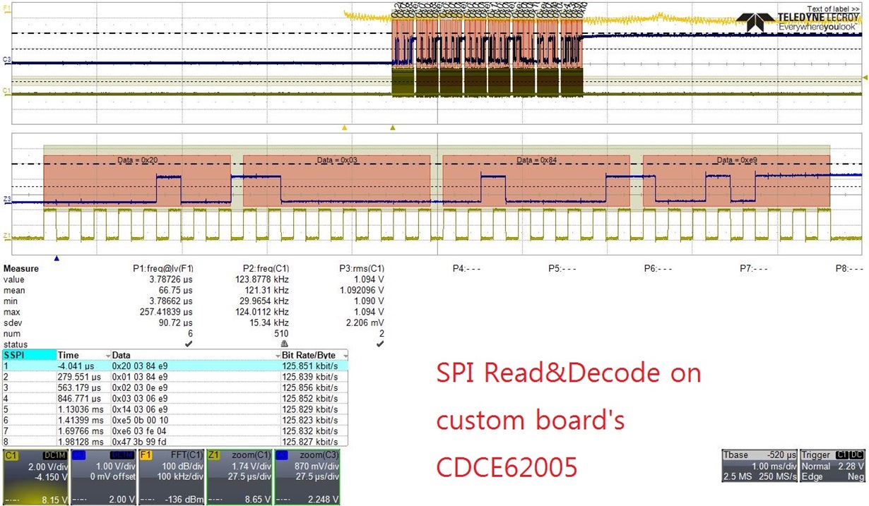
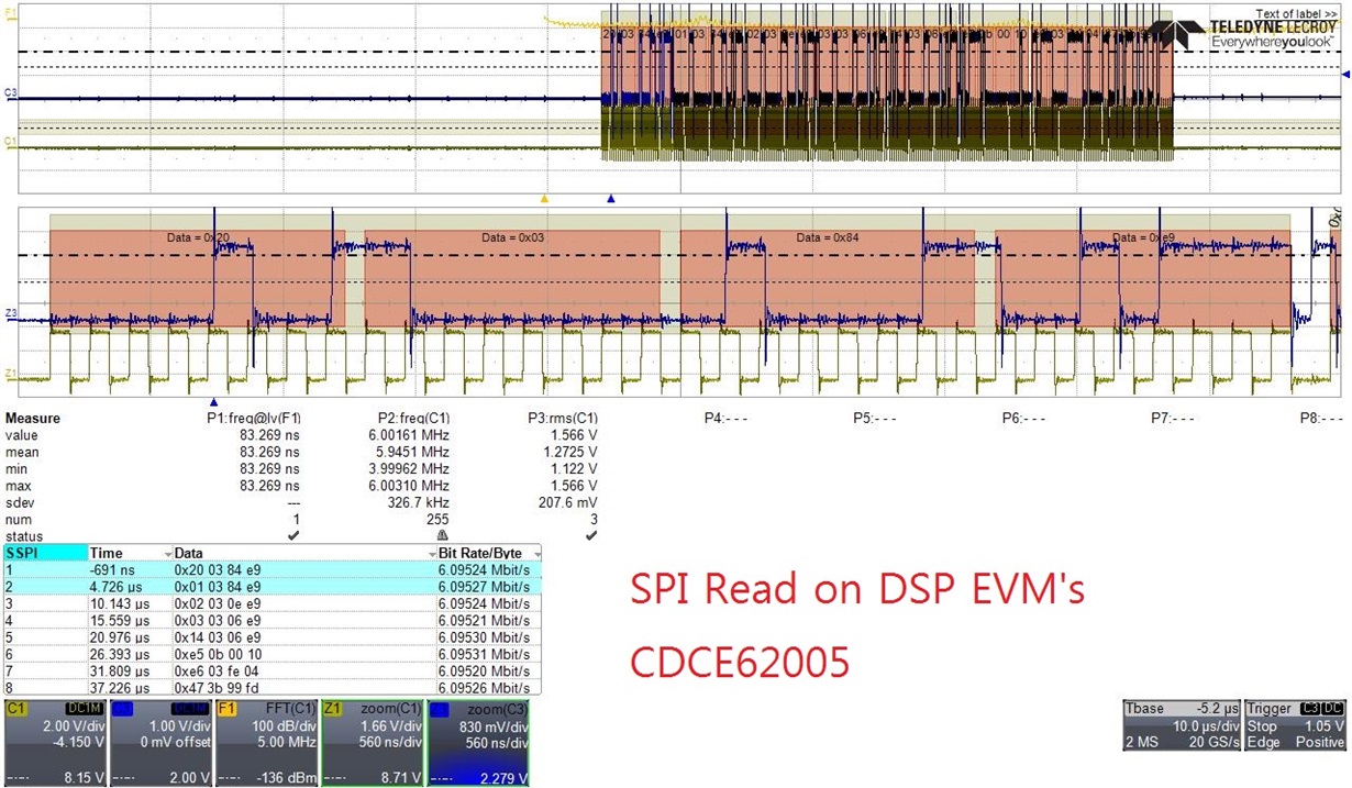
    I am attaching 2 DSO measurements from both DSP EVM and my custom board for your reference. If you find any clues, please kindly let me know.

    As for the possible SPI timing as you mentioned, I have checked the SPI timing and didn't find any possible errors with it. Besides, I would like to tell you that the values of the registers are always correct at their address values as well at the 8th register's value. I believe  that if there is timing error, I won't be able to read these values, or some random values will be received and the address bits won't be correct. But that was not the case. 

    I will purchase some new CDCE62005 chips to check the issue again.

    Thank you and good week.

    David