This thread has been locked.

If you have a related question, please click the "Ask a related question" button in the top right corner. The newly created question will be automatically linked to this question.

LMX2581: VCO Calibration Time - takes much too long !

Part Number: LMX2581
Other Parts Discussed in Thread: , CODELOADER

We are using the LMX2581 over a wide range with a comparably small step size, f=0.9-1.8 and 1.8-3.6 GHz, step df= 1-2kHz.

We have noticed distinct frequency regions where the VCO calibration time takes unusually long, in some regions few ms in

one very pronounced region up to 10 ms!

With VCO pre-selection calculated and programmed by our control software and CAP_CODE=47 the usual lock

time is <100us, seen in the Lock Detect signal and of course as seen easily with the spectrum analyzer in Zero-Span Mode

when the ICs AUTOMUTE function is on.

I have monitored the tuning voltage with an oscilloscope. With FCAL active its range is somewhere between slightly above 1.4V

down to around 1.2V.

From my observation, obviously, when FCAL kicks in during frequency change, there is a fixed voltage applied to the

VCO tuning pin, that is Vtune gets slightly below 1.4V and stays constant  for a short time (few 10 us).

The critical frequency range - the one with prolonged FCAL times is exactly in this region, where its corresponding

tuning voltage is also slightly below 1.4V.

The H/W is pretty much identical to the EVAL Board, Loop filter 5th order, 30 kHz bandwidth and CPG=24.

Any ideas ? Thank you in advance.

Cheers,

Konstantin

Dresden, Germany

  • Dresden,

    The first thing I would try to do is determine if this increased time is due to VCO calibration time or analog settling time.

    If you reduce the charge pump gain to say 4X, the loop bandwidth will decrease significantly and this will significantly increase the analog settling time, but it has no impact on the VCO calibration time. So if you see a huge increase, this implies this is dominated by the loop settling time, which means increasing the loop badnwidth might help. On the other hand, if the increase is only very small, then this implies that perhaps this is the VCO calibration time dominating.

    Another thing you can do is trying to enable the NO_FCAL bit if your frequency is close. This helps to see if it is analog PLL lock or the VCO calibration.

    Regards,
    Dean
  • Hello Dean,

    thank you for you rapid response. I fact I did check before - the problem is not caused by the analogue loop lock time.

    The delay is not occuring for all frequency points but only for certain (periodic) frequency sections.

    Little variation for changing the CPG  value. It seems to me it is the FCAL procedure.

    Note that we are observing VERY long times between two indicated lock states - several ms usally,  but we had today even up to 300ms !

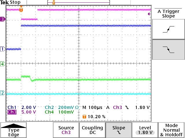
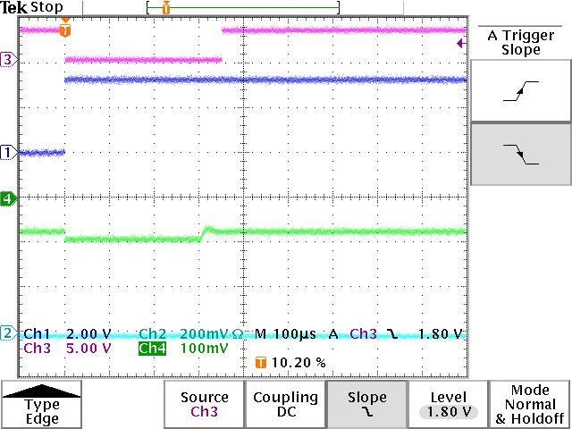
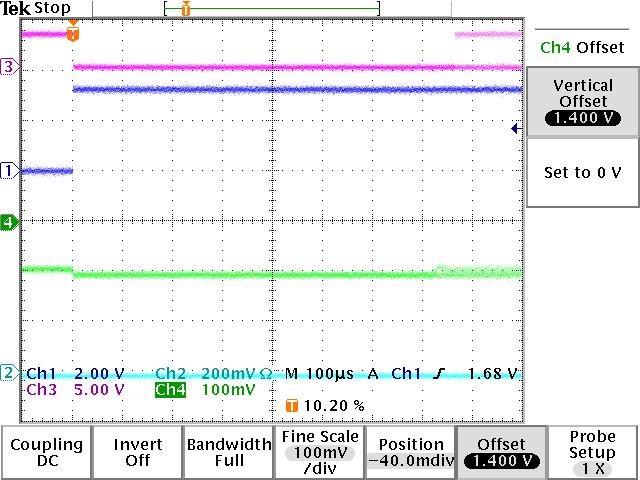
    To illustrate I am attaching 3 files.

    ch3 - purple - Lock Detect Signal (LD)

    ch1 - blue - Chip Select (CS)

    ch4 - green - Vtune

    A) In the normal case, we see, after the rising edge of CS, the LD (purple) is going low for about 100us and then high again. Thats fine.

    Note the tuning voltage goes to some sort of more or less fixed reference when FCAL starts - seen in the first part of the second

    graph division (green trace).

    B) Every time in the sweep, when Vtune comes close to this voltage, the time with LD=Low increases.

    See 350us here. That's only few MHz away from case A)


    C) Now thats a very bad state - LD stays low for several ms. Note Vtune.

    D) We have experimentally found, that adding a resistor of  10-15 kOhm

    parallel to the 1 uF capacitor at pin 22 (VrefVCO) partly improves the problem.

    E) We have checked our control test S/W program (Python via USB-to-SPI convertor)

    with your LMX2581-EVAL board. Similar effect but slightly less delay (still, 10ms have

    been seen also). I think I can exclude some mayor error in our H/W.

    Our questions are as follows:

    1) Has someone else observed similar effects with FCAL?

    2) What settings (if applicable) do you recommend to mitigate the effect?

    3) We are going to use the part with step sizes of 1-2 kHz. Sweep time is very critical in the application.

    Would it be OK to run the FCAL procedure only once every 1-2 MHz? That is we switch

    it off for around 1000 points and then on for only time and off for the next 1000 points and so forth.

    Could you recommend such algorithm?

    4)  Could you recommend operation with the mentioned 15kOhm resistor?

    Thank you very much for your support! Looking forward to hear from you soon.

    Cheers,

    Konstantin

    (Dresden, Germany)

  • Konstantin,

    1) We have not observed this effect nor heard this from other customers.

    2) A few things about settings:
    a. About a year after we released the LMX2581, we changed the programmable settings of regsiters R9 and R10. Just want to make sure that you have this.
    b. Maybe something with the VCO calibration. For instance, changing the VCO_SEL might mitigate this, especially if you can attribute this to when the VCO switches between cores. When you switch between cores, some of the LDO voltages on chip slightly change, so it might matter what direction. I also say this because you see some benefit of a 15k resistor.

    3) The VCO bands might be on the order of 20-30 MHz wide. Now we do need a lot of margin if you expect the temperature to drift significantly after locking and you don't do FCAL, but 1-2 MHz is pretty reasonable to do without calibrating, especially if you are not expecting a wide change in temperature after you do FCAL.

    4) We have never tried or experimented with the 15kohm nor seen the need, but if it works for you, seems reasonable. I suspect you might also try to look at VregVCO pin. Perhaps there is something about the value or characteristics (like ESR) might matter. We use ceramic capacitors, which have low ESR, but maybe something about your capacitors are too low or too high ESR.

    I say this because VregVCO and VrefVCO are both output pins of the internal LDO of the LMX2581 and if putting a 15kohm load seems to help, it suggests maybe something LDO related.

    Regards,
    Dean
  • Hello Dean,

    good to hear from you. We are surprised -  no one has measured that effect yet ?!

    For the reason, we have repeated the test with the TI evalaluation board - LMX2581EVM.

    H/W: original state, only thing we added is R32 (0 Ohms) - in order to make the lock detect signal available at the uWire 52601-S10-8LF connector.

    S/W: our Python based tool, PC - USB - FT2232H MiniModule - SPI - LMX2581EVM

    Procedure: After initialisiation we are generally programming only Reg0 (once) for each point. Reg1, Reg2 and Reg3 are only written when necessary (prior to Reg0).

    Fixed parameters: CPG=24, FL_TOC=10, FL_CPG=31, FRAC_ORDER=2, FRAC_DITHER=0, CAPCODE=47 ,OUTA_PWR=16, OUTB_PD=1, VCO_DIV=2

    Sweep: 910-1899 MHz output (with VCO_DIV2 that is 1820-3798 MHz core frequency), 10 kHz step, FCAL for each point.

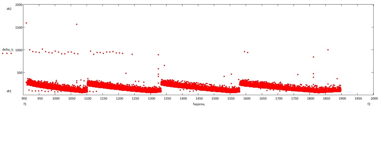
    Here are the results:

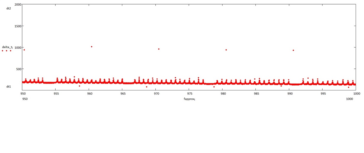
    x-axis: output frequency in  [MHz], y-axis: frequency change time (time for which LD= low) in [us].

    We can clearly see the 4 VCO ranges. The switching happens at pre-determined frequencies based on Table5 in your data sheet. Note that parameter VCO_SEL is matched for

    every frequency point and its register Reg1 is re-written when required. We also observe delays of up to 1.5 ms and numerous delays around 1ms. Please disregard the lowest

    points around 100 us (these are due to the measurement principle).

    There is also a periodicity, as I have described in my previous message. Whenever the tuning voltage is similar to the applied voltage during calibration the effect is observed.

    Here is a plot of a narrow range below 1 GHz:

    What goes on here ?

    Concerning your comment about Reg9 and Reg10 - we are using data sheet SNAS601G  (AUGUST 2012–REVISED SEPTEMBER 2014). Is that correct?

    By the way it seems there is an error on page 29 of the document. The allocation of  FL_INV is at bit 22. However, the Codeloader S/W writes it at position bit 25,

    which looks more logical considering the other grouping (we do write it as the Codeloader S/W).

    Please, could you pass this data to the IC designers of the part? May be someone in that group has an idea.

    Unfortunately, for our sweep application, total ramp time is very critical and this problem comes up at a time when we are almost ready with the system and

    it brings a lot of problems.

    We hope TI can help here!

    Cheers,

    Konstantin

  • Konstantin,
    1. Datasheet september 2014 is correct.
    2. I am using TICSPRO, but Ill look into this bit.
    3. I have been in contact with the designer, but .had no insights to add to this

    I tried this in the lab. First I tried 20 MHz steps up and then down the whole VCO range. Then did 1 MHz steps up and down the range. Then tried 10 kHz steps, but only in 20 MHz band as I didn't have automation.
    In any case, I didn't see the issue.

    I was looking at the Lock detect and set this to Digital lock detect and was looking at the negative pulse on the oscilloscope.

    REgards,
    Dean