This thread has been locked.

If you have a related question, please click the "Ask a related question" button in the top right corner. The newly created question will be automatically linked to this question.

TPL5110: DONE Signal Glue Logic Circuit

Part Number: TPL5110
Other Parts Discussed in Thread: TPL5111, , TPS63050

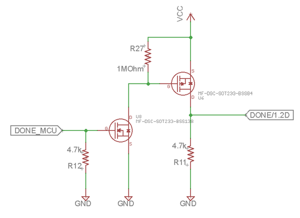
It seems to me like it might be a more robust and simpler approach (than what I've seen in the TPL5111 application notes) to idle the DONE signal to a high state rather than a low state. I've devised the glue logic circuit below to achieve this outcome. With this circuit, the microcontroller has to drive it's "DONE" output HIGH and then LOW to request a timer shutdown.

My thinking here is that this topology will be less susceptible to a glitch during system power up (further inhibited by the passive low pass filter on the output stage. the circuit also serves the purpose of isolating the battery voltage domain (VCC in the schematic below) from the system power domain where the MCU signals resides.

Hoping someone from TI can review this design decision and weigh in on whether there are any significant downsides to this approach?

  • Hi Victor,

    The DONE logic on the left is OK, but I'm not certain if the DONE logic on the right is acceptable. TPL5110 expects the low-high transition after the DRV falling edge, with a minimum tDdone spec of 100ns (see table 6.6).

    Kind regards,
    Lane

  • I am suggesting that in order to induce a shutdown with my circuit, the microcontroller would induce action to generate the signal on the right, by stimulating the input on the left. As such the TPL5110 would get a low-high transition at the trailing end of that sequence.

    t_DONE is required to have a minimum pulse width of 100ns (merely implying that the HIGH state has to persist for at least 100ns to register as a rising edge), per the Electrical Characteristics table in section 6.5. It's not actually at all clear to me what tD_DONE is meant to constrain. It is described as "DONE to DRV delay" with bounds of { min: 100ns, max: t_DRV } from DRV falling edge. To me that means that from the time a rising edge is presented on DONE, DRV will be re-asserted HIGH no less than 100ns and no more than t_DRV ns after the DRV goes LOW, subject to the a LOW to HIGH transition on DONE.

    While the timing diagram depicts the an idle state of the DONE signal as LOW, I am asking whether that is in fact _required_, because I think it would be more reliable design to have it idle in a HIGH state to prevent false-positive DONE signals during startup, at the expense of having to issue a HIGH to LOW transition followed by a LOW to HIGH transition on DONE to request a shutdown. I am happy to guarantee some minimum time the DONE signal must be low before the rising edge, but I don't see a description of that in the datasheet (maybe that's what tD_DONE is meant to constrain, and it's at least 100ns?).

    I appreciate your honesty with regard to not being certain. Please can you help me find someone in the TI engineering organization who can answer with certainty?

  • Terribly sorry, I said TPL5110 but I meant TPL5111 which is what I'm actually using. Sorry if that caused any confusion. Can someone please re-categorize the question title?

  • Hi Victor,
    We didn't verify a wide pulse on done as you did. It looks like not violate datasheet description. I suggest you could reserve a path to bypass this inversion circuits. And let us know your final test result in a new post in E2E. Thanks for your hard work on TPL5111.

    Regards,
    Shawn
  • Shawn,

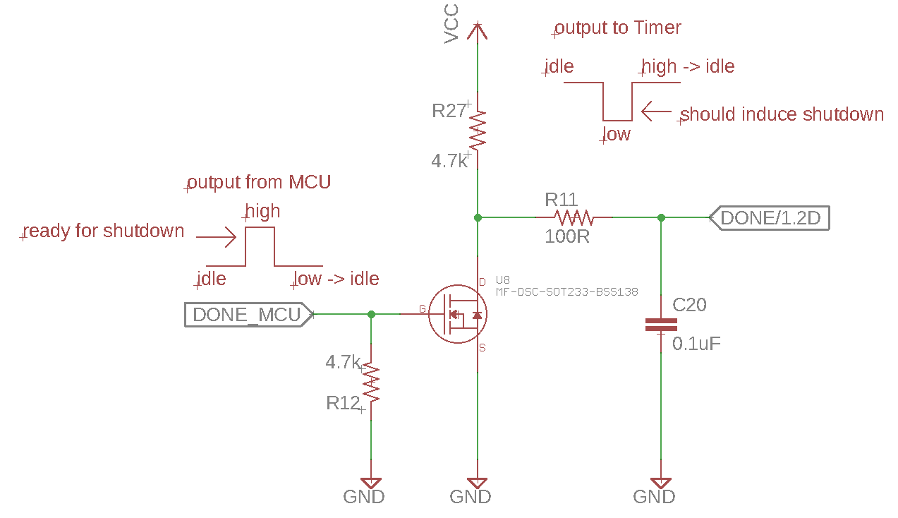
    Let me take a step back here. The circuit that I propose at the start of this thread is actually a _change_ I'm considering to the following circuit, which I have currently implemented and am having a subtle problem with.

    VCC in the diagram above is the battery voltage and ostensibly could be anything from 2.5 to 4.5V, but for testing I'm using a 3V power supply output. DONE_MCU comes from a microcontroller whose power comes from the TPS63050 output configured to for 3.3V. The DRV signal of the TPL5111 is connected, through a simple passive R-C filter (100 ohms / 100nF), to the EN input of the TPS63050. At its core, the problem I'm trying to address with the proposed change is a spurious DONE signal happening (cause unknown) very infrequently (<1% incidence) at the TPL5111 DRV -> HIGH event, giving rise to a meta-stable periodic condition in my system that looks like this at the output of my regulator (TPS63050). 

    bad state

    When I saw that on the regulator output, I probed the DONE input to the TPL5111 and saw this (blue trace):

    bad detail

    That little (360mV) runt pulse is pretty much perfectly correlated with the meta-stable regulator output waveform (yellow), but I can't wrap my mind around its origins, or its behavior.

    If it's genuinely triggering the DONE event in the TPL5111 (and disabling the TPS63050) it doesn't make sense that the metastability is ~72ms periodic, as I have the TPL5111 configured for a 10 minute wake interval.

    I don't see a way that the microcontroller would be causing that DONE signal to rise at startup as my firmware is trivial for this test, which literally waits 10 seconds, then configures the DONE_MCU pin as output and starts toggling it at 500Hz to request a shutdown. So where else could it be coming from? If it is that spurious DONE signal causing the problem, which I guess I'm not totally convinced of, I thought maybe floating it HIGH would be a way to eliminate it, but I've also considered putting passive R-C filters on the the TPL5111 DONE and M_DRV inputs. It's obviously also possible that the "real" problem here has nothing to do with the TPL5111 and everything to do with the TPS63050, but I don't see it if that's the case.

    If none of this adds up to you folks either, maybe we could take it offline for a design review? Awaiting further advice.

  • Hi Victor,

    The amplitude of the runt pulse is very small. It doesn't appear to cross the logic threshold.
    First thing I want to understand is the TPL5111 behavior. How are you forcing this behavior (runt pulse train on DONE)?
    Could you capture the DRV output in the same plot? It would also be helpful to see DRV -> HIGH waveform, and maybe the VDD waveform.

    We could also support a design review offline if you prefer. Please send us an email at clock_support@list.ti.com.

    Kind regards,
    Lane
  • Lane,

    Sadly, I have not yet found a way to purposefully induce the failure mode, it happens very rarely, and it clears spontaneously lasting an unpredictable amount of time. Pretty close to a worst case scenario for debugging :-). So it's quite difficult for me to capture the DRV output in the same plot, but I'll try. I can certanily capture the DRV -> HIGH waveform under normal operating conditions, though. By the VDD waveform do you mean the "battery" voltage (input to TPS63050) or the "system" voltage (output from TPS63050, that is what the yellow trace is in the pictures above)?

    Re: design review, are you guys equipped to review EAGLE CAD design files directly or would you prefer PDF?
  • Victor,

    Thanks for the information. By VDD I mean the battery voltage powering TPL5111.
    I would prefer PDF for the review

    Kind regards,
    Lane
  • Lane, just a heads up, I've emailed PDFs to clock_support@list.ti.com per your suggestion.
  • This is pretty interesting, I wired up the following signals to the scope and captured a power up event:

    VDD - output voltage of the TPS63050

    DONE - Done signal at input to the TPL5111

    ENABLE - DRV output of the TPL5111 at input to the TPS63050

    PG - Power Good signal output of the TPS63500

    That's 200us per division and 1V per division on all channels.

    One change I'm going to make in my next revision is to wire the Power Good output to the (active low) RESET pin of my microcontroller for good measure. That aside, what I'm curious about is why the DRV output of the TPL5111 decays from the time it comes up until the TPS63050 power good signal comes up, before charging back up to it's ultimate steady-state value. That is pretty peculiar. Is the TPS63050 dragging the drive signal down while it bootstraps, do I need to buffer the DRV output of the TPL5111? That would be a pretty lame requirement from a power consumption standpoint. Do I need to add capacitance to the signal?

  • More time to discuss off line.