This thread has been locked.

If you have a related question, please click the "Ask a related question" button in the top right corner. The newly created question will be automatically linked to this question.

LMK00105: Schematics For review

Part Number: LMK00105

Hi,

Please help me to review the schematics of LMK00105. 

Our Target application is as follows,

We have one 1PPS LVCMOS (3.3/2.5) signal comes from GPS receiver and we want to split this 1PPS signal to 2 LVCMOS 1.8V signal.

What all LVCMOS terminations have to be given  and  how to decide?..

  • Hello Vishnu,

    Since the signal is close to DC (1PPS), AC-coupling the CLKIN pin is not a good idea unless the pulse is very narrow (<1ms). Datasheet Figure 7 shows how to configure the LMK00105 input for DC coupling if needed. If J16 input sees 50Ω in series, the CLKIN pin sees VPP/2 maximum voltage swing at DC. The CLKIN* pin should be DC biased to the midpoint of this swing, or at VPP/4 volts. The bias resistors setting this midpoint can be in the range of 1-10kΩ. It looks like you have already chosen bias resistors in this range, and the values look acceptable. Note that if AC-coupling is used, these bias resistors are not needed and can be unpopulated.

    LMK00105 CLKOUT pins have 50Ω series terminations built-in, so external series resistors are not needed.

    If the downstream devices (CLKGEN and FPGA) have internal 50Ω input terminations, and the downstream devices can tolerate 0.9V directly on the clock inputs, the CLKOUT lines can be directly connected to the device clock inputs. If the devices do not have internal 50Ω termination, place 50Ω termination close to the input pin of the device.

    Other notes: Make sure to place bypass capacitors close to VDD rails. R766 should not be populated, and R767 can optionally be omitted, to ensure that CLKIN is the driving source.

    Regards,
  • Hi @Derek Payne,

    Thanks for your reply.

    The 1PPS signal is coming from the GPS receiver. The LVCMOS input may be of 3.3, 2.5,1.8 levels. Changing the resistors according to the logic is not possible. So how can we modify the scheme in order to work in all these specified levels of LVCMOS.
  • Hi Derek,

    What is it limiting us from AC coupling the input when it's PPS signal with significant pulse width?

    Regards,
    Shashank
  • Hello Shashank,

    I realize that my terminology should be clarified, because what I said is not strictly accurate. With 1 PPS, or with any other low frequency, AC-coupling begins to be a problem if the time between edges is larger than the time constant of the AC-coupling on the input. So more accurately, as the duty cycle tends toward 50% (worst case), low frequency inputs will have more trouble with AC-coupling. Wide pulses with high duty cycle, or narrow pulses with short duty cycle, will be less of a problem.

    When a low frequency input is AC-coupled, the voltage at the CLKIN pin will settle to the common-mode by the time the next edge arrives. This limits the magnitude of the voltage swing, and consequently makes it difficult to achieve the required slew rate. Refer to the datasheet, figure 1 and figure 2: as the input slew rate is reduced, the noise floor and the resulting RMS jitter both increase. This is because the transition edge is much harder to determine when the input has enough time to settle to the common mode voltage.

    On the other hand, if the pulse width is very short, the second edge of the signal will occur before the CLKIN pin settles to the common-mode voltage, allowing almost the full LVCMOS swing. Since the swing is larger, the input slew rate is faster, and the noise floor and resulting RMS jitter will be lower. Note that if the timing of the second edge on the 1 PPS input is not stable, then very high or very low duty cycle still does not provide much benefit for AC-coupling. This is why I suggest DC-coupling: if only one edge on the 1 PPS signal is stable, it does not matter if that edge is the rising or falling edge in a DC-coupled configuration.

    Vishnu,

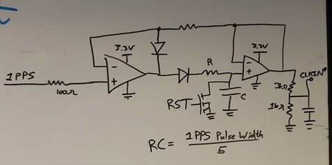
    Given that the signal is slow, you may be able to use a dual, high input impedance, rail-to-rail output op amp as a peak detector for your input signal:

    This method could run into issues with noise susceptibility if the PPS signal sees a glitch, but if the 1PPS is a clean signal this may work. I included a reset switch, which can be any high impedance open collector or open drain input, for if the input signal changes amplitude for any reason.

    If a 3.3V DAC is available on a system microcontroller, processor, etc, this could also be used as long as the PPS receiver input voltage is known or sensed beforehand. This is reconfigurable and uses fewer components, but that still leaves the problem of sensing the PPS signal level.

    I have asked another applications engineer to look into this as well. We will update this thread if we can come up with a simpler solution.

    Regards,