Hi,
I use CDCI6214 provide clock for FPGA,and Ouptut Format is LVDS 3.3V.
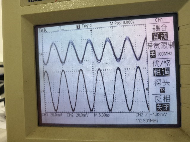
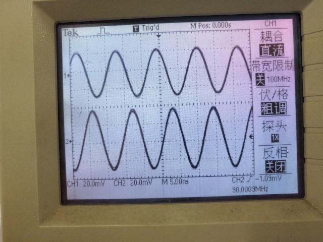
But the output clock is incorrect,Including peak, jitter and frequency of waveform.
This is waveform of Channel 2; My target frequency is 100MHz and the output buffer format is LVDS_3.3V.
This is waveform of Channel 3; My target frequency is 90MHz and the output buffer format is LVDS_3.3V.
This is waveform of Channel 4; My target frequency is 90MHz and the output buffer format is LVDS_3.3V.
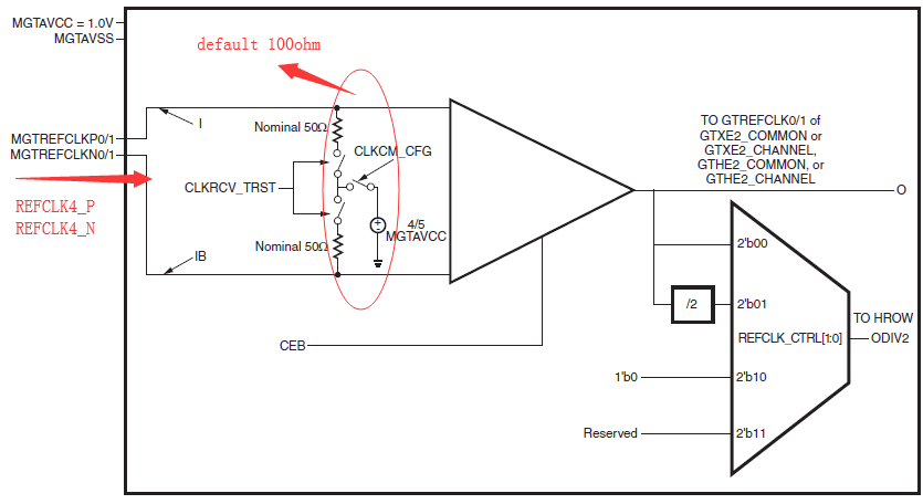
The circuit diagram is as follows:
RC15 and RC18 is removed. RESETN is connected to MCU.
I don't know what the problem is or what to do. Someone can help me.


