This thread has been locked.

If you have a related question, please click the "Ask a related question" button in the top right corner. The newly created question will be automatically linked to this question.

LMK05028: LMK05028 application issue

Part Number: LMK05028

Hi,

When we click the 'Run Script' button, the GUI would give below remind: OUT(0:3) bank needs 1+ clock from PLL2.

Is that mean we must select PLL2 for one output from OUT0~3? seam it's not same as the disription in dataheet.

Can you help to check and give some comments?
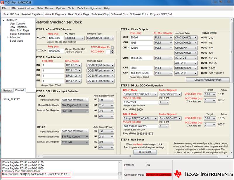
Tahnks.

  • Hello Oliver,

    Page 5 of datasheet for OUT0 to OUT3 under Pin Functions mentions that OUT[0:3] bank requires at least one clock from PLL2 domain if enabled.

    Can you advise the portion of the datasheet which is contradicting?  Or perhaps you feel this should have been included/made more apparent in the 9.3.10 clock distribution section or block diagram?  Thanks for your input.

    73,
    Timothy