This thread has been locked.

If you have a related question, please click the "Ask a related question" button in the top right corner. The newly created question will be automatically linked to this question.

WEBENCH® Tools/CDCI6214: Alternative for CDCI6214 filter design

Part Number: CDCI6214

Tool/software: WEBENCH® Design Tools

Hi,

I'm checking if the actual config. of CDCI6214 clock generator in our project is correct.

I have 2 questions:

  1. We are programming it in factory using CDCI6214EVM and Register Content Transfer from a .txt in TICS pro. Is it the correct way to program it or some field are device-specific and should be determined by TICS pro after each connection and calibration?
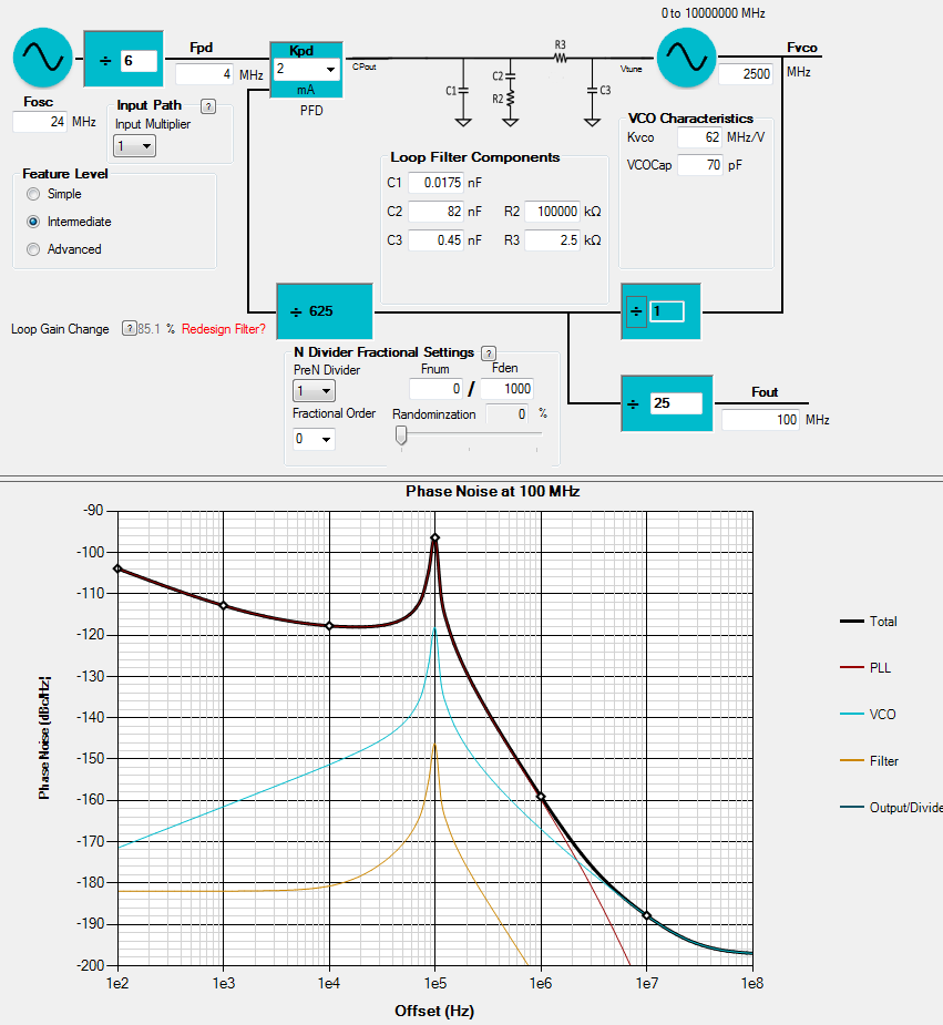
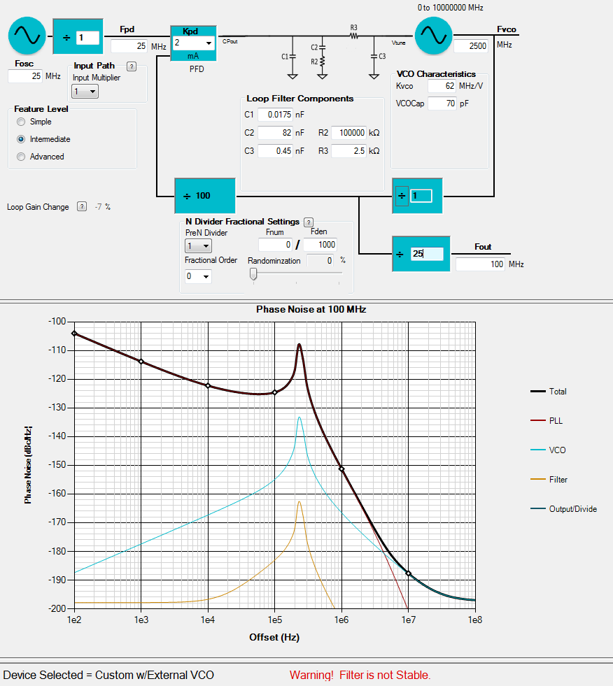
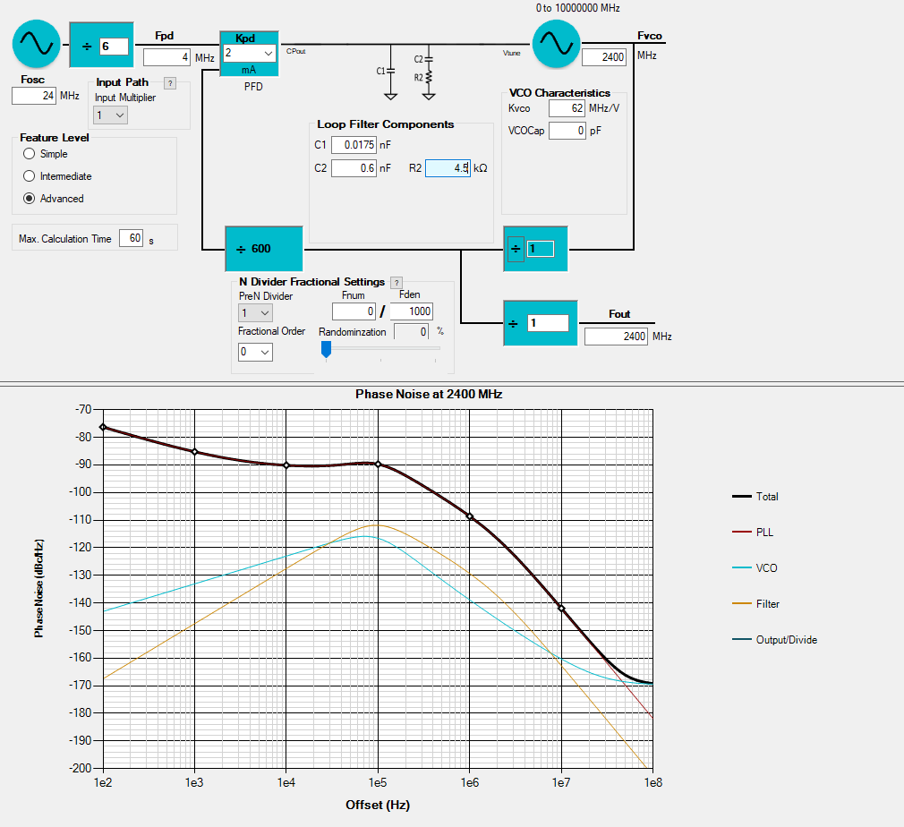
  2. I don't know if the actual configuration was done based upon some TI tools or not. I'm checking if it's correct. I've seen that in a thread of this forum the "WEBENCH clock architect" was suggested: this JAVA-based product has been discontinued by TI from Jan 31th 2020. Which other tool should I use to define VCO and PFD parameters to be sure that the BW and phase margin is as suggested in datasheet? I tried Platinum SIM but It doesn't have the CDCI6214 in the list: should I use a custom component. It keeps throwing an exception when I click in any menu: is it a actually supported tool?

Thank you.

  • Hi Giacomo,

    Yes it is OK to load the .txt hex register file to Ticspro directly -- in Ticspro, go to Select device -> clock generator / jitter cleaner (single loop) -> CDCI6214. Then in the tool bar, go to File -> import hex register values.

    For CDCI6214, default loop filter setting is sufficient for almost all use cases. Default setting can be loaded in Ticspro -- in the tool bar, Default Configuration -> fallback default.

    As for VCO frequency, PFD and so on, you can watch this video for basic clock frequency calculation: https://training.ti.com/ti-precision-labs-clock-and-timing-system-design-considerations-frequency-planning-part-1?context=1139747-1140114-1140118-1139974

    Eventually, the PLL needs to be "locked" after RECAL button is clicked -- below image shows a counterexample.

    Also attaching Ticspro user manual: TICS PRO GUI - User Manual.pdf

    Regards,
    Hao

  • Thank you for reply/

    We didn' t Re-CAL each unit because we thought that the recalibration would be done at chip start: is this uncorrect?

    I checked the video but it's very basic: in TICS pro (and table 2 of datasheet) there are some preset: currently we select "VCO 2400/PFD 25 / BW 0.51" preset but we have actually changed it to f_VCO=2500MHz, f_PFD=4MHz, f_out=100MHz so I must be check the phase margin and BW are okay with the current setup. I tried this set up in PLLatinumSIM  and it says it's unstable (see PPlatinumSIM and TICSpro screenshot attached).

    NOTE: I did manage to make PLLatinumSIM to work only selecting Windows regional setting = English (USA).

    NOTE: I selected 3rd order filter with R2 BIG to minic the filter represented in the datasheet, fig 19;

    NOTE: I left default VCOCap because it's not present in datasheet;

    Then I tried also the original "VCO 2400/PFD 25 / BW 0.51" pre-set with f_VCO=2400MHz, f_PFD=25MHz and it says it's unstable too (see other PPlatinumSIM screenshot attached).

    Which is my error? How should I check if the setup is correct (I attached our TICS pro setup)

    MODIFIED PRE-SET:

     .

    ORIGINAL PRESET:

    Thank you for support.

    Giacomo

  • Hi Giacomo,

    CDCI6214 has a 2nd order loop filter, where C1 is the pole cap and C2 is the zero cap. R2 is zero res. As an example:

    As for CDCI6214 VCO calibration, if EEPROM is used then the device will auto calibrate when it powers up from the device. Otherwise, if the device is programmed via I2C, then after all registers are programmed, you need to write a 1 to the recal bit.

    Regards,
    Hao

  • Thank you so much Hao for support.

    Some other doubts:

    1. the datasheet requires that RESETN is LOW until VDD is stable within 95%. Which supply is intended for VDD? In our setup we supply the chip with 2.5V (VDDREF, VDDVCO, VDDO12) and, after some time, 1,8V (VDDO34). Is it necessary to keep RESETN LOW until all voltage supplies are stable and not only VDDREF?
    2. is we don't use GPIO1,4 (not connected externally) is it ok to keep them as input set as IGNORE or change them to output?
    3. we are warned not to overwrite RESERVED reg. field: but I've found some RESERVED register default values that are different from those generated by graphical selection on TICSpro. Which is the correct approach with reserved fields? Can we trust TICS pro values OVER the datasheet? We actually used txt directly generated by TICS pro; e.g. POWER0 register bit 0 is RESERVED but:
      • 0x000400DD on PAGE1 default on ds -> bit 0 = 0
      • 0x00040055 on config selcted with TICSpro -> bit 0 = 1
    4. potential typo: the register reset value of GENERIC1 is 0x00016A32 (as in title of 8.6.1.2) or 0x00016832 (as suggested in table 67)?
    5. potential typo: the register reset value of CHX_CTRL0 is 0x003B0061 (as in tile of 8.6.1.51 of ds) or 0x003B0079 (as suggested in table 67)?

    Thank you again.

    Giacomo.

  • Hi Giacomo,

    Please see my comments below:

    1. VDD pins are VDDREF and VDDVCO and do not include VDDO12 and VDDO34. Only VDDREF needs to reach 95% of its final value but both VDDREF and VDDVCO need to ramp up within 2ms.

    2. Yes they can be set as ignored input

    3. When there's conflict, please refer to datasheet. For the above example, EEPROM page 1 corresponds to "PCIe 2x OE" in Ticspro default configurations, and R4 for both is 00DD. Between EEPROM page 0 and page 1, page 0 is 0x55 (0101 0101) and page 1 is 0xDD(1101 1101). The differences are bit 7 and bit 3. bit 7 is ch4 powerdown and bit 3 is ch2 powerdown. This is because by default channel 2 and channel 4 are powered down in EEPROM page 1.

    4. It should be 6832

    5. It should be 79