This thread has been locked.

If you have a related question, please click the "Ask a related question" button in the top right corner. The newly created question will be automatically linked to this question.

LMK04828-EP: LMK04828 PLL1 not locking

Part Number: LMK04828-EP
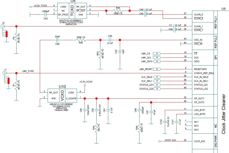
Other Parts Discussed in Thread: LMK04828, ADS54J60EVM, ADS54J60

We are having issues trying to get PLL1 to lock.  Attached is the TCS file used.  Regardless of using either an on board 10MHz source or external source PLL1 never locks.  The design is based upon the LMK04828EVM board.  

An interesting note...  when the device is placed in clock distribution mode and a 100MHz clock is applied to CLKIN1.  A clock output with no division is much less stable than the input.  The input is 0.5PPM stable however the output is 500PPM.  Also if the "divider only" option is selected the output drops to ~3.2MHz and doesn't really resemble a clock.

Any help would be appreciated.

Regards, GaryLMK04828 VCO0_2400MHz.tcs

  • Hello Gary,

    First, have you checked that the 10 MHz waveform has sufficient slew rate for the LMK04828? Usually this is applicable when a 10 MHz sine wave is used; the slew rate of a 3.3V single-ended sine wave is only 2π x F * Vpk = about 0.1V/ns, whereas the minimum slew rate recommended for LMK04828 inputs is 0.15V/ns. A clipped sine wave or CMOS square wave would likely be needed to achieve good performance at 10 MHz.

    Second, have you modified the loop filter from the LMK04828EVM board design? If so, please provide the values.

    Third, I see the format chosen is LVDS for the outputs. Have you modified the termination on the LMK04828EVM to support LVDS? Note that with AC-coupled LVDS, a 560Ω shunt resistor is required between the P and N terminals of each LVDS output for proper biasing at startup.

    I have tested your configuration in our lab, and I can see the expected frequency from both 10 MHz and 100 MHz. PLL1 and PLL2 lock on my board. I did see that when the signal power on the 10 MHz input was low (<12 dBm), PLL1 would not lock.

    Regards,

  • Derek,

    Thanks for your quick response.  I'm using custom hardware based upon the LMK04828 eval board.  The loop filter component values match the eval board.  The 10MHz clock applied to CLKIN0 is from a Abracon TCXO.  See attached image.  Will double check the slew rates.

    The 100MHz clock is applied externally.  The signal is a 1.8V LVCMOS square wave.  I'll have to double check the slew rate to ensure the device specs are being met.  Since the input is AC coupled I thought the minimum voltage is 0.25VPP.  Am I looking at the wrong parameter?

    After further investigation I could get PLL1 to lock sometimes by increasing the Phase Detector Frequency by reducing the input clock frequency, PLL 1 R divider and N dividers.  Is the previous fPD of 0.08MHz too low?

    I will double check the LVDS output terminations.

    Regards, Gary

  • Derek,

    We are using custom hardware that is largely based upon both the LMK04828EVM and ADS54J60EVM boards.  There are (2) ADS54J60.  The LMK04828 outputs (DLK_OUT_0, SDCLK_OUT_1, DCLK_OUT_2 and SDCLK_OUT_3) connected to the ADC54J60 CLKIN and SYSREF inputs.  Made the mistake of defining the output to be LVDS.  They should be LVPECL 2000mV.  The clock outputs going to the FPGA are defined to be LVDS.  Noticed on the ADS54J60EVM the LVDS outputs do not have the 560ohm shunt resistors.  We are using the 100ohm termination internal to the FPGA.  Would the incorrect output defined affect PLL operation?

    Wanted to confirm the characteristics for CLKIN.  As mentioned previously we are injecting a 100MHz LVCMOS (1.8V) signal.  If I'm looking at the correct parameter for our configuration the minimum is 0.25V and maximum is 2.4V.  Is this the correct parameter?  

    The design includes a Abracon 10MHz TCXO connected to CLKIN0.  Can't seem to configure the LMK04828 to have lock on PLL1 using this clock either.  The loop filter component values were selected to match the LMK04828EVM.  See the attached image which I previously missed.  

    Any feedback on the stability when using clock distribution mode and using a 100MHz clock input?  I found the result to be interesting.

    Any questions please let me know.  I look forward to your response.

    Thanks, Gary

  • Hi Gary,

    Your 1.8V LVCMOS signal coming in from CLKin1 is AC-coupled, so the signal swing you quoted is correct (0.25-2.4 Vpp) and your input meets the requirement. I'm guessing since it's LVCMOS that you have a good slew rate.

    If the LVDS going into the FPGA is AC-coupled, you should have 560Ω across the P/N terminals of the LMK04828 before the AC-coupling. Otherwise, if it's just directly connected to the FPGA's 100Ω termination, the 560Ω is not needed. Essentially, there needs to be a DC current path on startup between P/N in LVDS/HSDS mode, and that could also be the termination if there's no AC-coupling.

    As far as affecting operation, in some cases it would prevent the LVDS/HSDS from starting up correctly, and in the majority of cases it would delay startup. I don't think this is the issue you're encountering here based on your description, but it's good to cover all the bases.

    Based on the description of the TCXO in the vendor datasheet, the slew rate and signal swing should be sufficient. I don't think the input sources in either case are causing problems.

    For the PLL1 lock issues, I note that the 100 MHz VCXO datasheet specifies a minimum input resistance of only 10kΩ. Is it possible that the VCXO is loading the charge pump and causing the loop to become unstable? If you increase the charge pump gain (essentially the VCXO drive current) on PLL1, does the stability improve?

    For distribution mode, do you have a tcs file with that configuration? I can think of a few things that might affect the output stability such as the state of the SYNC_DISx bits (R324) and the SYSREF behavior, but if I have the register settings that could help narrow down the issue faster.

    Regards,

  • Derek,

    Thank you for your continued advice.  I did try to increase the charge pump gain.  Saw in another thread with a low phase detector frequency the charge pump gain should be increase.  Tried various settings but PLL1 still remains unlocked.

    Attached is the TCS file for clock distribution mode.  Wanted to note the output stability looks good with a 98MHz input clock.  However anything above the outputs are very unstable.  Strangely enough the div2 output (50MHz) output is solid.  

    Any incite is appreciated.

    Regards, GaryLMK04828 clock distribution 100MHz CLKIN1.tcs

  • Gary,

    DCLKoutX_DIV=1 is not a valid state for divider only mode, per the notes on table 17 and table 20 in the datasheet. To get 100 MHz output from 100 MHz input, the DCLKoutX_MUX should be set to bypass mode or to divider+DCC+HS mode. Typically the DCC circuit needs a higher clock distribution frequency to work well, so this may be part of the reason for the observed instability. I recommend setting the mux to bypass mode for divide ratio of 1.

    One other thing to check: if you change PLL1_WND_SIZE in the user controls page to 19ns instead of 43ns, do things improve on the VCO=2400MHz configuration?

    Regards,

  • Derek,

    I missed that note in the datasheet about using the divider only.  Was simply trying to get something expected from the device.  Ultimately we need to use a 100MHz input clock with outputs of 400MHz device clock and 3.125MHz sysref for the (2) ADS54J60 devices on board.

    I can try reducing PLL1_WND_SIZE to 19ns but won't that reduce the chances of achieving lock?  I would think the PLL1_WND_SIZE should be maximized while the PLL1_DND_CNT be minimized in an effort to achieve lock depending on the quality of the incoming clock?

    Thanks, Gary

  • Gary,

    When PLL1_WND_SIZE gets close to the period of the input clock, this can cause issues with the window detector. The window size varies a little from part to part and across voltage/temperature, but I don't think this should make a difference since you are well above the window detector size; it's just a quick test to eliminate that possibility.

    If you check the voltage at VCTRL on the VCXO when your 10 MHz is coming in, what do you see? Nominally I would expect the voltage to be at or near 1.65V. If the voltage is much lower (say below 1V), this points again to the input impedance of the VCXO. Alternately, if the voltage is much higher, the VCXO frequency may be off.

    Do you have access to the OSCout signals? Can you check if the VCXO is behaving properly from these signals?

    I have your unmodified configuration working on my lab setup with the same loop filter values and input resistor circuits. The only differences in our hardware setup are the PCB and the VCXO. I strongly suspect that the issue lies with the VCXO.

    Regards,

  • Derek,

    As you suggested I reduced the PLL1_WND_SIZE keeping in mind PLL1_DLD_COUNT to make sure I didn't constrict the incoming clock accuracy.  Didn't have an effect on PLL1 locking.

    Started to look at the VCXO.  Found a few interesting pieces of information.  Routed the PLL1_N signal to the Status_LD2 pin.  Also routed the PLL1_R signal to the Status_LD1 pin.  Found the PLL1_N pulse width varies slightly from time to time.  It isn't solid like the PLL1_R pulse width.  Using a counter the VCXO output is very stable.  The control pin was set to 0V by the controller.  However after the loop filter the clock is less stable.  Guessing the instability is causing the variation in the pulse width on PLL1_N.   The attached image shows the VCXO on CH1 and LMK04828_OSCIN_P on CH2.  Notice the noise on CH2 not present on CH1.

  • Hi Gary,

    I have just noticed that the OSCin* pin is shorted to ground. OSCin* if unused should be connected to ground through a 0.1µF capacitor. Shorting the unused pin directly to ground can cause issues with the OSCin buffer, which would explain the difficulty locking to PLL1.

    Regards,

  • Derek,

    Thank you for your continued support!  I didn't notice the missing capacitor either.  Is this something that you could confirm in your lab by tying the OSCin* to ground to check if either PLL will lock?

    We have obtained a LMK04828EVM to verify our register configuration with desired clock input and outputs.  Everything work as expected.  

    Our next plan is to use the 100MHz to drive the external CLKIN1 of the LMK04828EVM to create a 400MHz clock output.  The 400MHz clock would be applied to the custom ADC board with the 2nd LMK04828 operating in clock distribution mode.  In order for the 2nd LMK04828 produce a stable 400MHz the "clock output select" will be configured for Divider+DCC+HS.  Hopefully this will suit our needs.

    Let me know if you see an issue with this approach.

    Thanks!

  • Hello Gary,

    Unfortunately I did not have time to test the OSCin* to ground today, so I will have to get back to you on Monday with that answer.

    Regarding your configuration, there are two ways you could achieve the 400MHz to your ADCs:

    • Configure for bypass mode, and use the first LMK04828 to generate the 400MHz with clean duty cycle. Bypass mode skips the divider and the digital/analog delay blocks entirely, which can improve performance.
    • As you described, divide of 1 and Divider+DCC+HS mode. This allows the use of half-step and analog delay, which can be used to adjust the phase alignment of the clocks. If you do not need phase adjustment at the LMK04828 outputs, I recommend instead using bypass mode since there are fewer total stages to traverse and the noise performance should be better as a result.

    Regards,

  • Derek,

    Just an FYI.  We are using the LMK04828EVM to create the 400MHz to feed the 2nd LMK04828 with the back OSCIN* connection.  The 2nd LMK04828 is producing the clocks needed for the ADS54J60. 

    I'm sure you've better things to try but curious if you tried shorting the OSCIN* pin to ground to see if either PLL will lock.  

    Regards, Gary

  • Hello Gary,

    We won't have an opportunity to run this test in the near future. 

    Even if it does start up, we would not recommend this configuration of tying the OSCin* to GND

    Thank you,

  • Liam,

    Thanks for the follow up.  Given the events occurring the world I completely understand not trying the trivial check.  We do have a solution for us to continue working.  FWIW we are using 3rd party hardware that is based upon the ADS54J60EVM board although poorly implemented.

    Will mark the thread as resolved.  Stay safe!

    Regards, Gary