This thread has been locked.

If you have a related question, please click the "Ask a related question" button in the top right corner. The newly created question will be automatically linked to this question.

LMK03806: output of two LMK03806 cannot be fully synchronized

Part Number: LMK03806
Other Parts Discussed in Thread: LMK04806, LMK04832

Hi Sir,

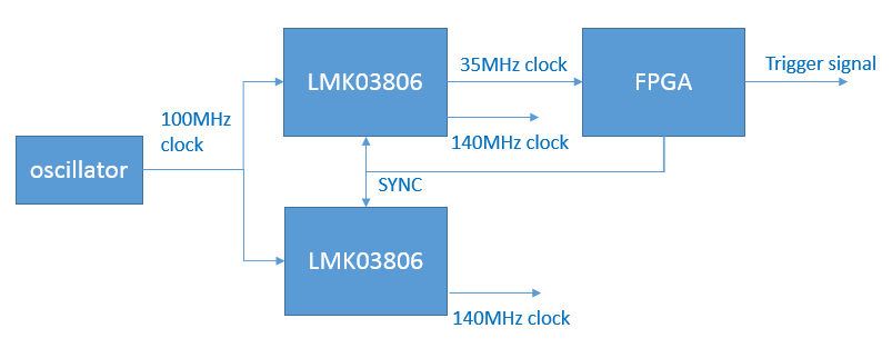
Below is a diagram of my design, as you can see I use the same FPGA pin to assert the "SYNC" signal of two LMK03806, so I am expecting the two 140MHz clock output are synchronized both in frequency and phase.

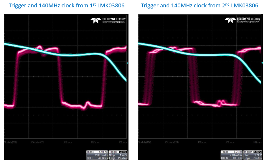
However, when I use the "Trigger signal" from FPGA as the triggering channel of oscilloscope, and measure the 140MHz clock from two LMK03806 separately, I found the 140MHz clock of the 1st LMK03806 synchronizes with trigger signal perfectly, however, obviously a ~0.4ns jitter can be observed on the 140MHz clock of the 2nd LMK03806.

Since the VCO inside LMK03806 is set to 2500MHz, 0.4ns is close to one clock period so I suspect there is something wrong on the SYNC mechanism, appreciated if there is any way to solve this problem, thanks !

  • Hello,

    I presume that if you triggered on both 140 MHz clocks, they would been phase and frequency locked without jitter?

    I presume that the trigger is occurring multiple times giving the visualization of the jitter of 0.4 ns?

    The SYNC of the LMK03806 will cause all the dividers on the single LMK03806 to reset. However the timing is not such that you could have assured phase relationship from LMK03806 input to output, or from LMK03806 to another LMK03806 less than a VCO cycle. Now the timing will be close. But it could be, as you have seen, a VCO cycle - perhaps even two off in timing over PVT.

    You may find that by changing the PLL charge pump value of the 2nd LMK03806 (which causes a timing change internal to the device) that you would get deterministic behavior, however this wouldn't be deterministic over PVT.

    --

    If the level of phase sync you have achieved is not acceptable, to achieve deterministic phase relationship between multiple devices, I recommend using 0-delay mode. Unfortunately the LMK03806 does not support 0-delay mode however the pin-compatible LMK04806 does.

    To use 0-delay, an output clock is fed back to the PLL2 phase detector instead of the feedback coming straight from the VCO. However there are some rules to achieve deterministic phase in a setup such as yours.

    1st) gcd(input clock frequency, output clock frequency) == input clock frequency
    2nd) a clock associated with the lowest frequency for which 0-delay synchronization is required must be used for feedback.

    In your case, if only the 140 MHz clocks must be deterministic with respect to each other:
    GCD(100 MHz, 140 MHz) = 20 MHz. So you must actually provide a 20 MHz reference when feeding back the 140 MHz clock to the PLL when clocked by a 100 MHz reference.

    If you wanted a high reference frequency, you could select 70 MHz.
    GCD(70 MHz, 140 MHz) = 70 MHz.

    If you wanted both 140 MHz and 35 MHz to be synchronized, I suggest a 35 MHz input clock.
    GCD(35 MHz, 140 MHz) = 35 MHz and
    GCD(35 MHz, 35 MHz) = 35 MHz.

    Of course this reduces you maximum phase detector frequency to the input clock. If a higher phase detector frequency is required for performance, the LMK04806 supports dual loop which would allow a VCXO at 100 MHz to operate with a 35 MHz reference. This will provide your system with the needed low frequency for phase synchronization and a high frequency reference for optimum PLL2 performance.

    73,
    Timothy
  • Hi Timothy,

    I presume that if you triggered on both 140 MHz clocks, they would been phase and frequency locked without jitter?

    >> yes, if I measure the 140MHz clocks separately, the 0.4ns jitter is gone.


    I presume that the trigger is occurring multiple times giving the visualization of the jitter of 0.4 ns?

    >> yes

    The SYNC of the LMK03806 will cause all the dividers on the single LMK03806 to reset. However the timing is not such that you could have assured phase relationship from LMK03806 input to output, or from LMK03806 to another LMK03806 less than a VCO cycle. Now the timing will be close. But it could be, as you have seen, a VCO cycle - perhaps even two off in timing over PVT.

    >> Do you mean the frequency of both 140MHz clock is the same, while their phase may deviate about 1 or 2 VCO cycle ? But if this is the case, on scope when I trigger the first 140MHz clock and measure the second 140MHz, I should not see jitter between the two clocks, instead a constant delay(1 or 2 VCO cycle) should be observed, though which is not the case in my measurement.

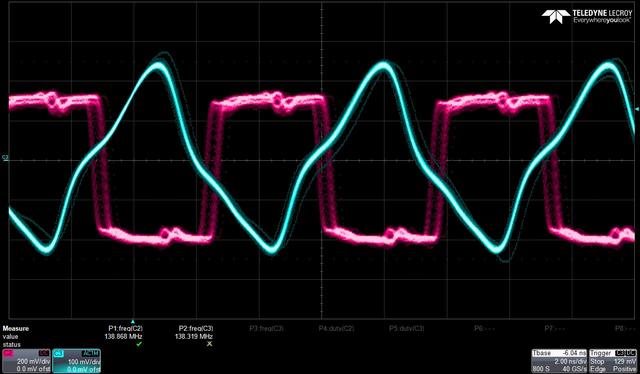
    blue : the first 140MHz clock (sorry I use a normal probe on this channel so shape of waveform is highly distorted)

    pink : the second 140MHz clock, a 0.4ns jitter can be observed with respect to the first 140MHz clock

    And thanks for the information of 0-delay mode of LMK04806, I will consider it.

  • Nate.Wang said:
    >> Do you mean the frequency of both 140MHz clock is the same, while their phase may deviate about 1 or 2 VCO cycle ? But if this is the case, on scope when I trigger the first 140MHz clock and measure the second 140MHz, I should not see jitter between the two clocks, instead a constant delay(1 or 2 VCO cycle) should be observed, though which is not the case in my measurement.

    What I mean is that from power-up to power-up there could be a cycle error.  Once locked, the phase will be fixed and constant.

    Another possibility for you is the LMK0482x or LMK04832.  There is a way to use it without dual loop had have deterministic phase  from power-up to power-up.  It has a SYSREF divider which can be used for 0-delay.  The divided SYSREF signal also clocks a D flip-flop which can have it's input driven by CLKin0 or SYNC (I suggest using CLKin0 for better timing).  This allow you to provide a 'SYNC' signal to the device which will be re-clocked by a lower frequency signal (SYSREF) that now has a phase relationship to the reference provided to OSCin because of 0-delay, this allows you to have divider reset determinism.  If you provide the a rising clock on CLKin0 on a falling edge of OSCin, then you can have your CLKin0 sync re-clocked onto the SYNC path and reset the dividers in multiple LMK0482x or LMK04832 devices at the same time.

    For cases where PLL2 R does not reduce to 1 with respect to your frequencies, the LMK04832 also allows synchronization of PLL2 R divider (and PLL1 R divider).

    73,
    Timothy

  • Hi Timothy,

    I am considering to replace the LMK03806 on board with LMK04806, but I am wondering the software compatibility from LMK03806 to LMK0486. It seems their register arrangement(R0~R31) is pretty the same. Do you know whether I can still use the same command sequence of LMK03806 for LMK04806 or some additional registers need to be configured to have LMK04806 working ? (of course I need to activate 0-delay mode of LMK04806)

    thanks.

  • Hello,

    You would be able to use the software pattern of the LMK03806, then add the needed registers.

    73,
    Timothy