This thread has been locked.

If you have a related question, please click the "Ask a related question" button in the top right corner. The newly created question will be automatically linked to this question.

CDCE62002 - SPI Command Structure

Guru 19775 points
Other Parts Discussed in Thread: CDCE62002

Hi Team,

I have a question about CDCE62002 SPI Command Structure.

You can find the SPI Command Structure and SPI Read/Write timing chart in the datasheet, but I cannot understand the bit relation between Figure 15/16 and Figure 17.

[Question 1]
What is the bitX relation between Data Field bits in Figure 17 and Figure15/16 ?
Please confirm if my recognition is correct.

<Figure 17>                 <Figure 15 or 16>
Data Field bit27     =    bit0
Data Field bit26     =    bit1
Data Field bit25     =    bit2
...
Data Field bit1       =    bit26
Data Field bit0       =    bit27

[Question 2]
What is the bitX relation between Figure17 Addr Field and Figure15/16 ?
Please confirm if my recognition is correct.

<Figure 17>             <Figure 15 or 16>
Addr Field bit3    =    bit24
Addr Field bit2    =    bit25
Addr Field bit1    =    bit26
Addr Field bit0    =    bit27

Best Regards,
Kawai

  • In the SPI command sequence, the command bitstream must include 32 bits, with LSB transmitted first.

    For write command, the bitstream starts with the 4-bit address field to be written (LSB first) followed by the 28-bit data field (LSB first).
    For read command, the bitstream starts with the read command (Addr[0:3]=0111) followed by the 28-bit data field where Data[0:3] is the 4-bit address of the register to read and Data[4:27] = zeros).

    Bit0 = Addr[0]
    Bit1 = Addr[1]
    ...
    Bit4 = Addr[3]
    Bit5 = Data[0]
    Bit6 = Data[1]
    ...
    Bit30 = Data[26]
    Bit31 = Data[27]

    Regards,
    Alan

  • Hi Alan-san,

    Thank you for the answer.  I am clear now.
    * I apologize that I had typo in my question, however it was wrong, I meant Address Field were Bit 28-31.

    Please let me ask you one more question.

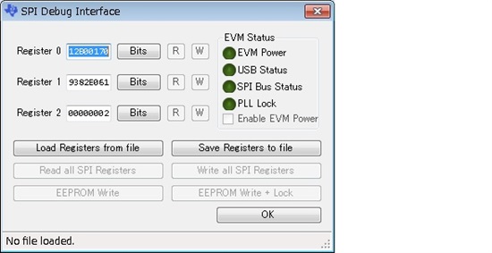
    When you describe the data in HEX code such as "0x12B00170" in the GUI window below, this data in binary code would be,

    "0001 0010 1011 0000 0000 0001 0111 0000"

    When reading this bit inforamtion, do you follow SPI Command structure in Figure 17 ?

    I am understanding as the following.

    0001 0010 1011 0000 0000 0001 0111            0000
    ^^^^^^^^^^^^^^^^^^^^^^^^^^^^^^^^^^^^^^^^^^            ^^^^^^
    MSB ---------- <Data Field> ----------- LSB          MSB-LSB (Address Field)

    Best Regards,
    Kawai

  • Yes, your understanding is correct.

    Regards,

    Alan

  • Hi Alan-san,

    I understood, thank you very much.

    Best Regards,
    Kawai