This thread has been locked.

If you have a related question, please click the "Ask a related question" button in the top right corner. The newly created question will be automatically linked to this question.

CDCM7005 PLL doesn't lock

Other Parts Discussed in Thread: CDCM7005

Hi,

We use a CDCM7005 to generate multiple clocks out of a 1GHz VCXO and 10MHz reference clock.
We initialize Word 0 with 0x3E4 and Word 2 with 0xDA4D0CA2 to set P=4, M=250, N=1.
Word 1 and 3 remain with their default values.
While STATUS_REF and STATUS_VCXO are high (the LEDs are ON) the PLL_LOCK stays low (the PLL is not locked).
What could the issue?
Is the CDCM7005 supposed to generate an output on the Y0-Y4 if the PLL is not locked? I suspect not but couldn't find a clear answer.
I attached the schematic we use.

Thanks,
Valentin

  • With P = 4, N should be 250 and M should be 1. Otherwise the PFD won't see the same frequency on the input reference path and feedback path.

  • Sorry typing error. N should be 25, M should be 1 when P = 4.

  • The correct value for N should be 25 indeed. We change word 0 to 0x60 but still have the same issue.

    We now suspect the IC we have on our board and will try to get a new one on the board.

  • We did replaced the CDCM7005 on our board but the issue will remain the same - the PLL doesn't lock.

    I am pretty sure I can communicate properly with the part because I checked it with a logic analyzer and I am also able to power down / power up the part by writing to word 2 bit 28.

    Any ideas what could be the issue?

  • It could be with the input or VCXO signaling level. The CDCM7005 supports single ended inputs only and can support differential or LVCMOS VCXOs. The VCXO input buffer on CDCM7005 is LVPECL type and so you can use the traditional 130 ohm (to Vcc) and 82 ohm (to GND) resistor network to interface via AC coupling (for LVDS VCXO) or DC coupling (for LVPECL VCXO).


    For LVCMOS VCXO, you need to bias N with 130 ohm (to Vcc) and 82 ohm (to GND). The VCXO LVCMOS output swing should be reduced to less than 2V and then AC coupled to the 130 ohm (to Vcc) and 82 ohm (to GND) network before typing to VCXO_IN_P pin.

  • As VCXO we use ASG-P-V-A-1.000GHZ which is a LVPECL VCXO that is DC
    coupled to CDCM like it is seen in our schematics (we posted our schematics at the beginning of this thread).
    We do use 130 ohm 82 ohm network between VCXO and CDCM.
    The VCXO datasheet is here http://www.abracon.com/Precisiontiming/ASG-P.pdf
    The measured DC level on both LVPECL lines is at 2V.

    The Primary Reference has LVCMOS and the datasheet is here: http://www.conwin.com/datasheets/tx/tx356.pdf

    It is really unfortunate there is no read-back from CDCM7005 that would give more info about what is wrong.

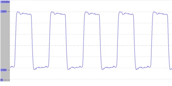
  • The Connor Winfield TCXO that you use as a reference to CDCM7005 has a rise/fall time of 8ns. The CDCM7005 only works with 4ns max. Can you select a different reference which has a faster rise time?

  • Yes, we could use another TCXO - hopefully we can find one with the same footprint. Thanks.

  • We did replace the TCXO with this one:

    http://www.abracon.com/Oscillators/AST3TQ.pdf

    The result is that there is lock only on VCXO and no lock on reference in and no PLL lock.

    The reference in lock pin is at 1.3V while the circuit is powered properly from 3V3 and I can see the 10MHz reference clock at cdcm7005 pin.

  • The amount of current draw from V3P3CLK is around 300mA for cdcm, vcxo and reference clock.

  • You loop filter is not optimal and doesn't have enough phase margin. What loop bandwidth do you want to set? I can help you pick the right values.

  • At this point we only care about getting something out of cdcm7005 as our project is in hold because we can not generate any output from cdcm7005

    We use the CDCM7005 to generate the clocks for a GSPS ADC and DAC (we need to provide 1000MHz clocks to both of them) and we also need 166MHz and 200MHz clocks. At this time we just try to get this up and running with the components we have on board. You can pick a PLL bandwidth that is feasible and will work for the above scenario and will give us low jitter. The PLL locking time is really not that important in our case.

  • I will try this tomorrow but I have a question: shouldn't we have the STATUS_REF pin high independent of the lowpass filter values? Do you have any explanation for the 1.3V voltage at the STATUS_REF pin?

    I am not sure how changing the filter will fix STATUS_REF issue.

  • One more question: Is there a way I could bypass the VCXO and just have the CDCM7005 like a clock buffer of the reference in? This will help us in bring-up our hardware.

    Or is there any other way to have the CDCM7005 generating output clocks without being locked?

  • Hello Valentin,

    providing the input reference to the outputs is not possible.

    What you could try, until you solved the issues with the TCXO...  a blue wire from another clock ( which fits the VCXO_IN pin requirements) to the VCXO inputs. The CDCM7005 can be used as a "clock buffer" and just create several copies on the outputs.

    Best regards,

    Patrick

  • Hi Patrick,

    Cool idea! Do I need any special settings in the registers for this to work as in this case the PLL will not be locked obviously but I will have clock generated on the output?

    Isn't this the same like disconnecting (or connecting it to a fix voltage) the voltage control pin out of the VCXO?

    Thanks,

    Valentin

  • We implemented the new loop filter - same issue. STATUS_VCXO is at 3.3V, STATUS_REF is at 1.3V (I checked this on the scope), PLL_LOCK is at 0V. The most puzzling thing is the 1.3V (DC) on STATUS_REF pin.

    We set word 0 to 0x60 and word 2 to 0xDA4D0CA2 and the other registers are at default values.

    Could I use undocumented GTME bit 16 in word 3 to do some on board testing of CDCM7005?

    How sensible is this chip to ESD? We do have ESD soldering station but one never know.

  • Hello Valentin,

    the status VREF 1.3V looks somehow like VCC-2V BIAS. Could it be there is some reference or measurement issue?

    I will check your schematic again and decode your settings as a crosscheck.

    Unfortunately I cannot share the reserved bits.

    One more question for my clarification: You mentioned you can see the reference clock at the device input. What about the outputs? Even if not locked (yet): do you see the outputs switching as programmed? Can you reset and powerdown the device repeatedly? Is the VCXO signal stable and does the new part achieve the required slew rates at the device ?

    Best regards,

    Patrick

  • Hello Valentin,

    please let me know if you were able to solve your issue.

    Thanks!

    Best regards,

    Patrick

  • Hi Patrick,

    No, we have not solved the issue - we are wondering if we should search another clock generator - we just can not get enough info from this part to understand what is going on.

    We replaced the CDCM7005 again and that fixed the STATUS_REF issue - we have this at 3.3V now so both the VCXO and the reference are locked - however there is no PLL_LOCK.

    We believe the P,N,M values we had initially are not valid - can you please confirm this?

    We had P=4, N=1, M=25 but we believe the right values are P=4, N=25, M=1 for 1GHz VCXO and 10MHz reference, right? Vcxo/ref = PxN/M and we must have P=4 for the frequency applied to N divider to be smaller that 300MHz

    Yes, I see output switching as programmed.

    Yes, we can reset/power down the device repeatedly without any issues and it will always come up with lock on VCXO and reference but no PLL_LOCK.

    We didn't change the VCXO but the reference and the edges for reference looks good.

    Thanks,

    Valentin

  • Attached is the reference clock as it looks at the CDCM7005 pin. As seen in our schematics the reference is AC coupled into the CDCM7005 thru a 10k/10k divider.

  • Hi Patrick,

    Problem solved - I had to redesign the loop filter with a higher bandwidth taking in account the characteristics of the particular VCXO we use.

    Quite a struggle with this clock generator... I was wondering how many gates (or transistors) were saved by not implementing the read back functionality of the SPI registers?. That is useful when troubleshooting something as complex as a PLL were a lot could/would go wrong.

    Thanks for your help,

    Valentin

  • Hello Valentin,

    to my knowledge the original purpose of this device was very specific and high performance the goal. I hope you will find a more convenient part fitting your application from our catalog and all our newer parts with SPI or I2C always offer read-back functionality.

    Please feel free to contact us again when you have any doubts or need for clarification.

    Best regards,

    Patrick