This thread has been locked.

If you have a related question, please click the "Ask a related question" button in the top right corner. The newly created question will be automatically linked to this question.

LMK04906: LMK04906 strange behaviour after reprogramming with FPGA

Part Number: LMK04906

Hi,

Let us describe our problem. We have a board with FPGA and external PLL which is LMK04906.

We observe some strange behaviour during initialization phase of LMK04906. After power up, we have reset registers that are default for LMK04906. After power-up, FPGA enter User Mode and initializate external PLL (using LeuWire interface). External PLL configures successfully (we program PLL to work in single PLL2 Mode with internal VCO and choose proper output clocks, Phase Detector and other settings). It also configures successfully after powerup start from external flash. It also successfully reconfigures an infinite number of times from User Mode if we initiate that initialization from PC-JTAG interface. But (!!!) after reprogramming FPGA (without cold reset) with the same programming file with the same settings PLL initializes wrongly (!!!!!). It means that - 1. PLL didn't reset     2. All registers from 1 to 31 didn't change their values, except register 30, which rewrites wrongly!  (As we think, PLL after reconfiguration is insensible to rewrite registers R0-R29). That means that we are unable to reset PLL, because R0 value didn't chage.  

Also interesting thing is that if we even readback from PLL after first initialization and reprogram FPGA, then PLL initializes properly.  

Please help us with that issue!

Thank you very much in advance.

Best Regards,  

Ivan

  • I'm not sure the issue, it sounds like some programming issue in how the data is sent in the two different cases. Can you share the SPI plots between a success and failure programming?

    This doesn't necessarily align with your description of the problem, but there is the uWire_LOCK bit, R31[5]. If set you will locked out programming of the device until R31[5] = 0 again.

    73,
    Timothy
  • Hi Timothy!

    Thank you very much for your answer!

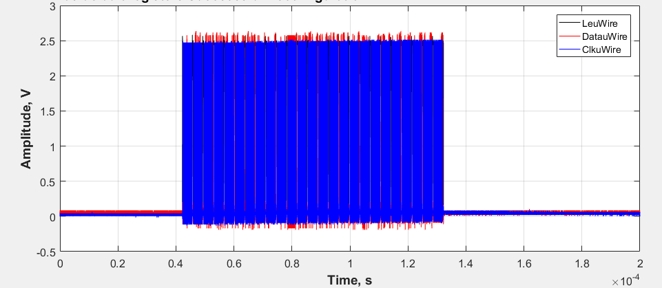
    We attached Matlab file (power_up_reconf__reinit_conf.fig)  which consists of  two graphs with CLKuWire, LEuWire and DATAuWire interface pins. There are prefixes -successfull \ -unsuccessfull.

    Successful plots are obtained with first LMK04906 ("PLL" thereafter) initialization, that means that after power-up,  the LMK04906 (PLL) contains reset (default) register values. As we enter User Mode in FPGA, we start to initialize the PLL according to our requirements (Single PLL mode, internal VCO and so on..). Register change list is attached (*.txt   file). LEuWire/CLKuWire/DATAuWire interface-pins behaviour was recorded and named accordingly with prefix "-successfull".

    After PLL was successfully programmed, we try to reprogram the FPGA with the same *.sof file (We use Altera FPGA and it is SRAM object file) that we used before, LEuWire/CLKuWire/DATAuWire interface-pins behaviour was recorded and named accordingly with prefix "-unsuccessfull"  (those are two graphs that presented in the attached MatLab figure). We compared them but seen no difference.

    As for uWire_LOCK bit we think that we never program it to value "1", it is always "0" value.

    Best regards,

    Ivan

    0640.registers_to_initilize_LMK04906.txt
    						--R0 (address(4..0) = "00000") - clk_out_0
    						register_array(0)(4 downto 0)		<= (others => '0'); -- address
    						register_array(0)(31)				<= '0';	-- clk_out_0 - power up
    						register_array(0)(30 downto 28)	<= (others => '0');	-- analog delay off
    						register_array(0)(27 downto 18)	<= std_logic_vector(to_unsigned(120,10)); --(p.56) digital delay 120 VCO clk periods 0-522
    						register_array(0)(17)				<= '0';	-- reset turn off
    						register_array(0)(16) 				<= '1';	-- digital delay HS0 (Even) - ref to p.38(table 8)
    						register_array(0)(15 downto 5)	<= std_logic_vector(to_unsigned(120,11));	-- for clk_out_0 = 17.5MHz (ADC1) (VCO 2450/140) p.58
    						--R1 (address(4..0) = "00001") - clk_out_1
    						register_array(1)(4 downto 0)		<= std_logic_vector(to_unsigned(1,5)); -- address
    						register_array(1)(31) 				<= '0';	-- clk_out_1 - power up
    						register_array(1)(30 downto 28)	<= (others => '0');	-- analog delay off
    						register_array(1)(27 downto 18) 	<= std_logic_vector(to_unsigned(120,10)); --(p.56) digital delay 120 VCO clk periods 0-522
    						register_array(1)(17) 				<= '0';	-- powerdown turn off
    						register_array(1)(16) 				<= '1';	-- digital delay HS1 - ref to p.38(table 8)
    						register_array(1)(15 downto 5)	<= std_logic_vector(to_unsigned(140,11));	-- for clk_out_1 = 17.5MHz (VCO 2450/140) p.58
    						--R2 (address(4..0) = "00010") - clk_out_2
    						register_array(2)(4 downto 0)		<= std_logic_vector(to_unsigned(2,5)); -- address
    						register_array(2)(31) 				<= '0';	-- clk_out_2 - power up because of SYNC_QUAL requirements p.63(Ethernet output clk)
    						register_array(2)(30 downto 28)	<= (others => '0');	-- analog delay off
    						register_array(2)(27 downto 18) 	<= std_logic_vector(to_unsigned(120,10)); --(p.56) digital delay 120 VCO clk periods 0-522
    						register_array(2)(17) 				<= '0';	-- must be 0
    						register_array(2)(16) 				<= '1';	-- digital delay HS2 - ref to p.38(table 8)
    						register_array(2)(15 downto 5)	<= std_logic_vector(to_unsigned(98,11));	-- for clk_out_2 = 25 MHz (VCO 2450/98) p.58
    						--R3 (address(4..0) = "00011") - clk_out_3
    						register_array(3)(4 downto 0)		<= std_logic_vector(to_unsigned(3,5)); -- address
    						register_array(3)(31) 				<= '0';	-- clk_out_3 - power up
    						register_array(3)(30) 				<= '1';	-- OSCin source
    						register_array(3)(29 downto 28) 	<= (others => '0');	-- analog delay off
    						register_array(3)(27 downto 18) 	<= std_logic_vector(to_unsigned(120,10)); --(p.56) digital delay 120 VCO clk periods 0-522
    						register_array(3)(17) 				<= '0';	-- must be 0
    						register_array(3)(16) 				<= '0';	-- digital delay HS3 (DIV Odd) - ref to p.39(table 8)
    						register_array(3)(15 downto 5)	<= std_logic_vector(to_unsigned(1,11));	-- for clk_out_3 = 100MHz (OSCin/1) p.58
    						--R4 (address(4..0) = "00100") - clk_out_4
    						register_array(4)(4 downto 0)		<= std_logic_vector(to_unsigned(4,5)); -- address
    						register_array(4)(31) 				<= '0';	-- clk_out_4 - power up
    						register_array(4)(30) 				<= '1';	-- OSCin source
    						register_array(4)(29 downto 28) 	<= (others => '0');	-- analog delay off
    						register_array(4)(27 downto 18) 	<= std_logic_vector(to_unsigned(120,10)); --(p.56) digital delay 120 VCO clk periods 0-522
    						register_array(4)(17) 				<= '0';	-- must be 0
    						register_array(4)(16) 				<= '0';	-- digital delay HS4 (DIV Odd) - ref to p.38(table 8)
    						register_array(4)(15 downto 5)	<= std_logic_vector(to_unsigned(1,11));	-- for clk_out_4 = 100MHz (OSCin 100/1) p.58
    						--R5 (address(4..0) = "00101") - clk_out_5
    						register_array(5)(4 downto 0)		<= std_logic_vector(to_unsigned(5,5)); -- address
    						register_array(5)(31) 				<= '1';	-- clk_out_5 - power down
    						register_array(5)(30 downto 28) 	<= (others => '0');	-- analog delay off
    						register_array(5)(27 downto 18) 	<= std_logic_vector(to_unsigned(120,10)); --(p.56) digital delay 120 VCO clk periods 0-522
    						register_array(5)(17) 				<= '0';	-- must be 0
    						register_array(5)(16) 				<= '1';	-- digital delay HS5 - ref to p.38(table 8)
    						register_array(5)(15 downto 5)	<= std_logic_vector(to_unsigned(50,11));	-- for clk_out_5 (VCO/10) p.58
    						--R6 (address(4..0) = "00110")
    						register_array(6)(4 downto 0)		<= std_logic_vector(to_unsigned(6,5)); -- address
    						register_array(6)(31 downto 28)	<= (others => '0');	-- must be 0
    						register_array(6)(27 downto 24)	<= std_logic_vector(to_unsigned(1,4)); --(p.58) clk_out_1 type - LVDS
    						register_array(6)(23 downto 20)	<= std_logic_vector(to_unsigned(1,4)); --(p.58) clk_out_0 type - LVDS
    						register_array(6)(19 downto 16)	<= (others => '0');	-- must be 0
    						register_array(6)(15 downto 11)	<= (others => '0');	-- analog delay clk_out_1 = 500ps + no delay
    						register_array(6)(10)				<= '0';					-- must be 0
    						register_array(6)(9 downto 5) 	<= (others => '0');	-- analog delay clk_out_0 = 500ps + no delay
    						--R7 (address(4..0) = "00111")
    						register_array(7)(4 downto 0)		<= std_logic_vector(to_unsigned(7,5)); -- address
    						register_array(7)(31 downto 28)	<= (others => '0');	-- must be 0
    						register_array(7)(27 downto 24)	<= std_logic_vector(to_unsigned(2,4)); -- clk_out_3 type - LVPECL p.58
    						register_array(7)(23 downto 20)	<= std_logic_vector(to_unsigned(8,4));	-- clk_out_2 type - LVCMOS (Norm/Norm) p.58
    						register_array(7)(19 downto 16)	<= (others => '0');	-- must be 0
    						register_array(7)(15 downto 11)	<= (others => '0');	-- analog delay clk_out_3 = 500ps + no delay
    						register_array(7)(10)				<= '0';					-- must be 0
    						register_array(7)(9 downto 5) 	<= (others => '0');	-- analog delay clk_out_2 = 500ps + no delay
    						--R8 (address(4..0) = "01000")
    						register_array(8)(4 downto 0)		<= std_logic_vector(to_unsigned(8,5)); -- address
    						register_array(8)(31 downto 28) 	<= (others => '0');	-- must be 0
    						register_array(8)(27 downto 24)	<= (others => '0');	-- clk_out_5 type - powerdown
    						register_array(8)(23 downto 20) 	<= (others => '0');	-- must be 0
    						register_array(8)(19 downto 16) 	<= std_logic_vector(to_unsigned(2,4)); --(p.58) clk_out_4 type - LVPECL
    						register_array(8)(15 downto 11) 	<= (others => '0');	-- analog delay clk_out_5 = 500ps + no delay
    						register_array(8)(10)				<= '0';					-- must be 0
    						register_array(8)(9 downto 5) 	<= (others => '0');	-- analog delay clk_out_4 = 500ps + no delay
    						--R9 (address(4..0) = "01001")
    						register_array(9)(4 downto 0)	<= std_logic_vector(to_unsigned(9,5)); -- address
    						register_array(9)(30)	<= '1';
    						register_array(9)(28)	<= '1';
    						register_array(9)(26)	<= '1';
    						register_array(9)(24)	<= '1';
    						register_array(9)(22)	<= '1';
    						register_array(9)(20)	<= '1';
    						register_array(9)(18)	<= '1';
    						register_array(9)(16)	<= '1';
    						register_array(9)(14)	<= '1';
    						register_array(9)(12)	<= '1';
    						register_array(9)(10)	<= '1';
    						register_array(9)(8)		<= '1';
    						register_array(9)(6)		<= '1';
    						--R10 (address(4..0) = "01010")
    						register_array(10)(4 downto 0)	<= std_logic_vector(to_unsigned(10,5)); -- address
    						register_array(10)(31 downto 28) <= std_logic_vector(to_unsigned(1,4)); -- must be 1
    						register_array(10)(27 downto 24) <= std_logic_vector(to_unsigned(1,4));	--(p.59) OSC_out type - LVDS
    						register_array(10)(23)				<= '0';	-- must be 0
    						register_array(10)(22)				<= '1';	-- OSC_out - enable (p.60)
    						register_array(10)(21)				<= '0';	-- must be 0
    						register_array(10)(20)				<= '0';	-- bypass divider OSC_out (p.60)
    						register_array(10)(19)				<= '0';	-- normal operation OSC_out (p.60)
    						register_array(10)(18 downto 16)	<= (others =>'0');	-- OSC_out divider = 8(but it was bypassed)
    						register_array(10)(15)				<= '0';	-- must be 0
    						register_array(10)(14)				<= '1';	-- must be 1
    						register_array(10)(13)				<= '0';	-- must be 0
    						register_array(10)(12)				<= '0';	-- no divide VCO (p.61)
    						register_array(10)(11)				<= '1';	-- must be 1 because of using dinamic digital delay
    						register_array(10)(10 downto 8)	<= (others =>'0');	-- VCO devider = 8(but it was bypassed)
    						register_array(10)(7 downto 5)	<= std_logic_vector(to_unsigned(3,3));	-- CLK_out_3 is selected as a reference output clock
    						--R11 (address(4..0) = "01011")
    						register_array(11)(4 downto 0)	<= std_logic_vector(to_unsigned(11,5)); -- address
    						register_array(11)(31 downto 27) <= std_logic_vector(to_unsigned(6,5));	-- (p.62) Single PLL mode, internal VCO
    						register_array(11)(26)				<= '1';	-- SYNC - enable, required for dinamic d.d. (p.62)
    						register_array(11)(25)				<= '1';	-- clk_out_5 will not be synchronized (p.63)
    						register_array(11)(24)				<= '1';	-- clk_out_4 will not be synchronized (p.63)
    						register_array(11)(23)				<= '1';	-- clk_out_3 will not be synchronized (p.63)
    						register_array(11)(22)				<= '1';	-- clk_out_2 will not be synchronized (p.63)
    						register_array(11)(21)				<= '0';	-- clk_out_1 will be synchronized (p.63)
    						register_array(11)(20)				<= '0';	-- clk_out_0 will be synchronized (p.63)
    						register_array(11)(19 downto 18)	<= (others =>'0');	-- should be logic low (p.63)
    						register_array(11)(17)				<= '1';	-- qualification by selected reference clock (clk_out_3)
    						register_array(11)(16)				<= '1';	-- SYNC is active low
    						register_array(11)(15)				<= '0';	-- SYNC auto off - manual mode
    						register_array(11)(14 downto 12) <= std_logic_vector(to_unsigned(0,3));	-- SYNC IO pin type (input)
    						register_array(11)(11 downto 6)	<= (others =>'0');	-- must be 0
    						register_array(11)(5)				<= '0';	-- XTAL disabled (p.73)
    						--R12 (address(4..0) = "01100")
    						register_array(12)(4 downto 0)	<= std_logic_vector(to_unsigned(12,5)); -- address
    						register_array(12)(31 downto 27)	<= std_logic_vector(to_unsigned(2,5));	-- PLL2 DLD (digital lock detect selection for LD pin)
    						register_array(12)(26 downto 24)	<= std_logic_vector(to_unsigned(3,3));	-- status_LD - output type
    						register_array(12)(23)				<= '0';	-- turning off as we use SYNC_QUAL = 1
    						register_array(12)(22)				<= '0';	-- turning off as we use SYNC_QUAL = 1
    						register_array(12)(21 downto 20) <= (others => '0');	-- must be 0
    						register_array(12)(19 downto 18) <= "11";	-- must be ones
    						register_array(12)(17 downto 9)	<= (others => '0');	-- must be 0
    						register_array(12)(8)				<= '0';	-- disable DAC for PLL1 tuning voltage
    						register_array(12)(7 downto 6)	<= std_logic_vector(to_unsigned(1,2));	-- holdover disabled (p.67)
    						register_array(12)(5)				<= '1';	-- must be 1
    						--R13 (address(4..0) = "01101")
    						register_array(13)(4 downto 0)	<= std_logic_vector(to_unsigned(13,5)); -- address
    						register_array(13)(31 downto 27)	<= std_logic_vector(to_unsigned(4,5));	-- asserting status_HO pin as "holdover status"
    						register_array(13)(26 downto 24)	<= std_logic_vector(to_unsigned(3,3));	-- asserting status_HO pin as output
    						register_array(13)(23)				<= '0';	-- must be 0
    						register_array(13)(22 downto 20)	<= (others => '0');	-- status_CLKin1 - logic low
    						register_array(13)(19)				<= '0';	-- must be 0
    						register_array(13)(18 downto 16)	<= std_logic_vector(to_unsigned(3,3));	-- asserting status_CLKin0 as output push-pull
    						register_array(13)(15)				<= '1';	-- diables the holdover mode from being activated because of PLL1 (p.68)
    						register_array(13)(14 downto 12)	<= std_logic_vector(to_unsigned(6,3));	-- status_CLKin0 - uWire readback
    						register_array(13)(11 downto 9)	<= (others => '0');	-- Clkin_select - CLKin0
    						register_array(13)(8)				<= '0';	-- status_CLKin0/status_CLKin1 is "active high"
    						register_array(13)(7 downto 5)	<= (others => '0');	-- CLKin0|1|2 are disabled (p.70)
    						--R14 (address(4..0) = "01110")
    						register_array(14)(4 downto 0)	<= std_logic_vector(to_unsigned(14,5)); -- address
    						register_array(14)(31 downto 30)	<= (others => '0');	-- setting time before loss-of-signal asserts (1200 ns)
    						register_array(14)(29)				<= '0';	-- must be 0
    						register_array(14)(28)				<= '0';	-- disable LOS detect (because this is for CLKin that we don't use)
    						register_array(14)(27)				<= '0';	-- must be 0
    						register_array(14)(26 downto 24)	<= std_logic_vector(to_unsigned(3,3));	-- status_CLKin1 type - output push-pull
    						register_array(14)(23)				<= '0';	-- must be 0
    						register_array(14)(22 downto 20)	<= (others => '0');	--	asserting CLKin buffers to be "Bipolar" for LVDS (p.71)
    						register_array(14)(19 downto 14)	<= std_logic_vector(to_unsigned(63,6));	-- high threshold of the voltage at which "Holdover mode" is entered
    						register_array(14)(13 downto 12)	<= (others => '0');	-- must be 0
    						register_array(14)(11 downto 6)	<= (others => '0');	-- low threshold of the voltage at which "Holdover mode" is entered
    						register_array(14)(5)				<= '0';	-- disables entering holdover mode dependency on DAC Vtune
    						--R15 (address(4..0) = "01111")
    						register_array(15)(4 downto 0)	<= std_logic_vector(to_unsigned(15,5)); -- address
    						register_array(15)(31 downto 22)	<= (others => '0');	-- asserting DAC value to 3.2 mV if in manual mode (p.72)
    						register_array(15)(21)				<= '0';	-- must be 0
    						register_array(15)(20)				<= '1';	-- selection of the DAC manual mode
    						register_array(15)(19 downto 6)	<= std_logic_vector(to_unsigned(512,14));	-- clocks before holdover mode (but holdover mode was disabled)
    						register_array(15)(5)				<= '0';	-- force holdover - disable
    						--R16 (address(4..0) = "10000")
    						register_array(16)(4 downto 0)	<= std_logic_vector(to_unsigned(16,5)); -- address
    						register_array(16)(31 downto 30)	<= (others => '0');	--	confirm that XTAL lvl is 1.65 Vpp (XTAL was disabled in R11)
    						register_array(16)(24)				<= '1';	-- must be 1
    						register_array(16)(22)				<= '1';	-- must be 1
    						register_array(16)(20)				<= '1';	-- must be 1
    						register_array(16)(18)				<= '1';	-- must be 1
    						register_array(16)(16)				<= '1';	-- must be 1
    						register_array(16)(10)				<= '1';	-- must be 1
    						--R24 (address(4..0) = "11000")
    						register_array(17)(4 downto 0)	<= std_logic_vector(to_unsigned(24,5));	-- address
    						register_array(17)(31 downto 28)	<= std_logic_vector(to_unsigned(0,4));		-- PLL2_C4_LF capacity (p.73)
    						register_array(17)(27 downto 24)	<= std_logic_vector(to_unsigned(0,4));		-- PLL2_C3_LF capacity (p.74)
    						register_array(17)(23)				<= '0';	-- must be 0
    						register_array(17)(22 downto 20)	<= std_logic_vector(to_unsigned(0,3));		-- PLL2_R4_LF resistance
    						register_array(17)(19)				<= '0';	-- must be 0
    						register_array(17)(18 downto 16)	<= std_logic_vector(to_unsigned(0,3));		-- PLL2_R3_LF resistance
    						register_array(17)(15)				<= '0';	-- must be 0
    						register_array(17)(14 downto 12)	<= (others => '0');	-- PLL1_N digital delay - 0 ps
    						register_array(17)(11)				<= '0';	-- must be 0
    						register_array(17)(10 downto 8)	<= (others => '0');	-- PLL1_R digital delay - 0 ps
    						register_array(17)(7 downto 6)	<= std_logic_vector(to_unsigned(3,2));	-- window size used for digital lock detect for PLL1 (p.76) 40ns - same as reset value
    						register_array(17)(5)				<= '0';	-- must be 0
    						--R26 (address(4..0) = "11010")
    						register_array(18)(4 downto 0)	<= std_logic_vector(to_unsigned(26,5));	-- address
    						register_array(18)(31 downto 30)	<= std_logic_vector(to_unsigned(2,2));		-- window size DLD must be 2
    						register_array(18)(29)				<= '0';	-- reference frecuency doubler bypassed (f_OSCin * 1)
    						register_array(18)(28)				<= '0';	-- internal VCO requires the negative charge pump polarity to be selected (p.77)
    						register_array(18)(27 downto 26)	<= (others => '0');	-- never mind as we are selecting TRI-STATE at PLL2_CP_gain
    						register_array(18)(25 downto 23)	<= (others => '1');	-- must be 1
    						register_array(18)(22)				<= '0';	-- must be 0
    						register_array(18)(21)				<= '1';	-- must be 1
    						register_array(18)(20)				<= '0';	-- must be 0
    						register_array(18)(19 downto 6)	<= std_logic_vector(to_unsigned(8192,14));	-- Number of PDF cycles which phase error must be within DLD window before LD state is asserted (p.78)
    						register_array(18)(5)				<= '1';	-- Entering TRI-STATE at PLL2_CP (loop filter)
    						--R27 (address(4..0) = "11011")
    						register_array(19)(4 downto 0)	<= std_logic_vector(to_unsigned(27,5));	-- address
    						register_array(19)(31 downto 29)	<= (others => '0');	-- must be 0
    						register_array(19)(28)				<= '1';	-- Many VCXOs use positive slope (p.78)
    						register_array(19)(27 downto 26)	<= (others => '0');	-- never mind as we are selecting TRI-STATE at PLL1_CP_gain
    						register_array(19)(25 downto 20)	<= (others => '0');	-- pre divider CLKinX = 1
    						register_array(19)(19 downto 6)	<= std_logic_vector(to_unsigned(96,14));	-- PLL1 divider (p.79)
    						register_array(19)(5)				<= '1';	-- Entering TRI-STATE at PLL1_CP (loop filter)
    						--R28 (address(4..0) = "11100")
    						register_array(20)(4 downto 0)	<= std_logic_vector(to_unsigned(28,5));	-- address
    						register_array(20)(31 downto 20)	<= std_logic_vector(to_unsigned(2,12));	-- PLL2_R = 2 - reference frecuency will be 50MHz (OSCin/2)
    						register_array(20)(19 downto 6)	<= std_logic_vector(to_unsigned(50,14));	-- PLL1 N devider
    						register_array(20)(5)				<= '0';	-- must be 0
    						--R29 (address(4..0) = "11101")
    						register_array(21)(4 downto 0)	<= std_logic_vector(to_unsigned(29,5));	-- address
    						register_array(21)(31 downto 27)	<= (others => '0');	-- must be 0
    						register_array(21)(26 downto 24)	<= "001";	-- OSCin freq >63 to 127 MHz (100MHz)
    						register_array(21)(23)				<= '0';	-- phase detector frecuency <= 100MHz
    						register_array(21)(22 downto 5)	<= std_logic_vector(to_unsigned(7,18));	-- PLL2_N_cal = PLL2_N = 7 (to reach PDF = 50MHz)
    						--R30 (address(4..0) = "11110")
    						register_array(22)(4 downto 0)	<= std_logic_vector(to_unsigned(30,5));	-- address
    						register_array(22)(31 downto 27)	<= (others => '0');	-- must be 0
    						register_array(22)(26 downto 24)	<= std_logic_vector(to_unsigned(7,3));	-- PLL2_P (prescale divider) = 7
    						register_array(22)(23)				<= '0';	-- must be 0
    						register_array(22)(22 downto 5)	<= std_logic_vector(to_unsigned(7,18));	-- PLL2_N = PLL2_N_cal = 7 (to reach PDF = 50MHz)
    						--R31 (address(4..0) = "11111")
    						register_array(23)(4 downto 0)	<= std_logic_vector(to_unsigned(31,5));	-- address
    						register_array(23)(31 downto 22)	<= (others => '0');	-- must be 0
    						register_array(23)(21)				<= '0';	-- LEuWire must be low for readback
    						register_array(23)(20 downto 16) <= std_logic_vector(to_unsigned(0,5));
    						register_array(23)(15 downto 6)	<= (others => '0');	-- must be 0
    						register_array(23)(5)				<= '0';	-- 1: R0-R30 locked| 0: R0-R30 unlocked

  • Failed to attach matlab file, uploaded it to Disk :  https://drive.google.com/open?id=0B2uQ-6QWshBJOHVBSHYxNjlSZWM

  • Hello, Timothy!

    We've found an interesting issue. After fist successfull initialization of the LMK04906 (PLL), we tried programming FPGA with *.sof file (We use Altera FPGA and it is SRAM object file)  which is the same as we used before except that we do not initialize PLL that time as we enter "User Mode" in FPGA and just wait for a readback command.

    More detailed, we write "readback address" bits R31(20 downto 16) with the successfull initialization and then program FPGA with the *.sof file that doesn't initialize PLL, so as we enter "User Mode" in the FPGA we try to read from the register (from the address that we recorded in the PLL before) and we get the values. As we find out, after exiting from the "User Mode"  (due to reprogramming with *.sof file) :

    As we started to check all the registers from 31 to 0 we found out that when we read form registers 31 - 16 we get zeros and from 15 - 0 registers have wrong values, except from register 0 (but only because register 1 and 0 have the same values). It turned out that as we read from 7th register we get values that shoud be in 14th (R14 -> R7), from 6th we get values that should be in 12th (R12 ->R6), from 5th we get values that should be in 10th (R10 ->R5) and so on... From 0 register we get right values probably because it consists exactly the same values as the 1st. 

    R1 (addr)    00001 -> 00000   R(0)

    R10(addr)   01010 -> 00101   R(5)

    R12(addr)   01100 -> 00110   R(6)

    R14(addr)   01110 -> 00111   R(7)

    As we said before, we use *.sof file that does not initialize PLL when entering "User Mode", so after PLL is programmed we can program that *.sof file (which skips initialization of the PLL) and readback from register addres writen earlier (last successful initialization of the PLL). Pll also may be reinitialized during the "User Mode" by consequent registers recording from reset (R0[17]) to R0-31 (we have a "repeat_initialization" parameter that initializes the PLL with required settings (those that PLL has after successful initializing). After geting correct register values written in the PLL, we can change "readback address" and reprogram FPGA with *.sof file that does not initialize PLL and get readback values from previously selected register.

    So after first reinitialization (without programming *.sof file, just repeating Registers sending to PLL - from reset (R0[17]) to R0-31).

    After first repeat_initialization we try readback second time and check all the registers again, R29-R0 this time have correct values, but R30-R31 are incorrect.

    After second repeat_initialization we try readback third time and check all the registers again, this time all registers have correct values.

    Best regards,

    Ivan

  • Hello, Timothy!

    We've found an interesting issue. After fist successfull initialization of the LMK04906 (PLL), we tried programming FPGA with *.sof file (We use Altera FPGA and it is SRAM object file)  which is the same as we used before except that we do not initialize PLL that time as we enter "User Mode" in FPGA and just wait for a readback command.

    More detailed, we write "readback address" bits R31(20 downto 16) with the successfull initialization and then program FPGA with the *.sof file that doesn't initialize PLL, so as we enter "User Mode" in the FPGA we try to read from the register (from the address that we recorded in the PLL before) and we get the values. As we find out, after exiting from the "User Mode"  (due to reprogramming with *.sof file) :

    As we started to check all the registers from 31 to 0 we found out that when we read form registers 31 - 16 we get zeros and from 15 - 0 registers have wrong values, except from register 0 (but only because register 1 and 0 have the same values). It turned out that as we read from 7th register we get values that shoud be in 14th (R14 -> R7), from 6th we get values that should be in 12th (R12 ->R6), from 5th we get values that should be in 10th (R10 ->R5) and so on... From 0 register we get right values probably because it consists exactly the same values as the 1st. 

    R1 (addr)    00001 -> 00000   R(0)

    R10(addr)   01010 -> 00101   R(5)

    R12(addr)   01100 -> 00110   R(6)

    R14(addr)   01110 -> 00111   R(7)

    As we said before, we use *.sof file that does not initialize PLL when entering "User Mode", so after PLL is programmed we can program that *.sof file (which skips initialization of the PLL) and readback from register addres writen earlier (last successful initialization of the PLL). Pll also may be reinitialized during the "User Mode" by consequent registers recording from reset (R0[17]) to R0-31 (we have a "repeat_initialization" parameter that initializes the PLL with required settings (those that PLL has after successful initializing). After geting correct register values written in the PLL, we can change "readback address" and reprogram FPGA with *.sof file that does not initialize PLL and get readback values from previously selected register.

    So after first reinitialization (without programming *.sof file, just repeating Registers sending to PLL - from reset (R0[17]) to R0-31).

    After first repeat_initialization we try readback second time and check all the registers again, R29-R0 this time have correct values, but R30-R31 are incorrect. It sholud be noticed that PLL does not reset during first repeat_initialization (it can be seen at readback pin, as default readback pin is "status_HO" and initialization selected readback pin is "status_CLKin_0").

    After second repeat_initialization we try readback third time and check all the registers again, this time all registers have correct values. Pll resets here, after second repeat_initialization process it could be seen that readback_pin changes for a time from reset bit (R0[17]) occures till we rich register which programms readback_pin to a new value.

    Best regards,

    Ivan

  • Can you provide images like .jpg, .png, etc of your plots? You will be able to attach these files... the other file is 145 Mbytes, so that's probably why our site wouldn't allow you to upload.

    73,
    Timothy
  • Hi Timothy!

    We attached a link to Matlab figure, and here is the link : https://drive.google.com/open?id=0B2uQ-6QWshBJOHVBSHYxNjlSZWM

    Picture (jpg, png and so on) resolution isn't enough to examine interface in detail.

    If you don't have Matlab, we can attach *.csv file or text file. But in taht case you would have to plot data yourself.

    Also please have a look at our last message :

    We've found an interesting issue. After fist successfull initialization of the LMK04906 (PLL), we tried programming FPGA with *.sof file (We use Altera FPGA and it is SRAM object file)  which is the same as we used before except that we do not initialize PLL that time as we enter "User Mode" in FPGA and just wait for a readback command.

    More detailed, we write "readback address" bits R31(20 downto 16) with the successfull initialization and then program FPGA with the *.sof file that doesn't initialize PLL, so as we enter "User Mode" in the FPGA we try to read from the register (from the address that we recorded in the PLL before) and we get the values. As we find out, after exiting from the "User Mode"  (due to reprogramming with *.sof file) :

    As we started to check all the registers from 31 to 0 we found out that when we read form registers 31 - 16 we get zeros and from 15 - 0 registers have wrong values, except from register 0 (but only because register 1 and 0 have the same values). It turned out that as we read from 7th register we get values that shoud be in 14th (R14 -> R7), from 6th we get values that should be in 12th (R12 ->R6), from 5th we get values that should be in 10th (R10 ->R5) and so on... From 0 register we get right values probably because it consists exactly the same values as the 1st. 

    R1 (addr)    00001 -> 00000   R(0)

    R10(addr)   01010 -> 00101   R(5)

    R12(addr)   01100 -> 00110   R(6)

    R14(addr)   01110 -> 00111   R(7)

    As we said before, we use *.sof file that does not initialize PLL when entering "User Mode", so after PLL is programmed we can program that *.sof file (which skips initialization of the PLL) and readback from register addres writen earlier (last successful initialization of the PLL). Pll also may be reinitialized during the "User Mode" by consequent registers recording from reset (R0[17]) to R0-31 (we have a "repeat_initialization" parameter that initializes the PLL with required settings (those that PLL has after successful initializing). After geting correct register values written in the PLL, we can change "readback address" and reprogram FPGA with *.sof file that does not initialize PLL and get readback values from previously selected register.

    So after first reinitialization (without programming *.sof file, just repeating Registers sending to PLL - from reset (R0[17]) to R0-31).

    After first repeat_initialization we try readback second time and check all the registers again, R29-R0 this time have correct values, but R30-R31 are incorrect.

    After second repeat_initialization we try readback third time and check all the registers again, this time all registers have correct values.

    Best regards,

    Ivan

  • Ivan Deyneka said:
    If you don't have Matlab, we can attach *.csv file or text file. But in taht case you would have to plot data yourself.

    Yes, please post the CSV file.

    73,
    Timothy

  • Hello Timothy!

    Here are two CSV files.

    Best regards,

    IvanCSV_interface.rar

  • Hi Timothy!

    Is there enough info about our issue at the moment? Do you need additional files?

    Best regards,

    Ivan

  • I started to review the files.  However they seem to be more  noise than programming?  I expected to see a well behaved clock with data along side and CS*.  Also the Y values are very low,   Is this supposed to be voltage?

  • Hello Timothy!

    Here is another CSV file (CSV_secondCSV_second.rar). The only difference is that three signals are now separated. The beginning of the file consists no valuable data, it looks like in the overall png attached. You probably inspected only that part of file.

    Best regards,

    Ivan

  • Hi Timothy!

    Have you reviewed our file?

    Best regards,

    Ivan
  • I'm afraid I've not you got a chance to review this. My plan is to decode your SPI data, then program the same into an LMK04906 to see the behavior.

    I'm not expecting anything to be fundamentally wrong, probably something simple with program or usage. As you have the one programming which works.

    73,
    Timothy
  • Hi Timothy!

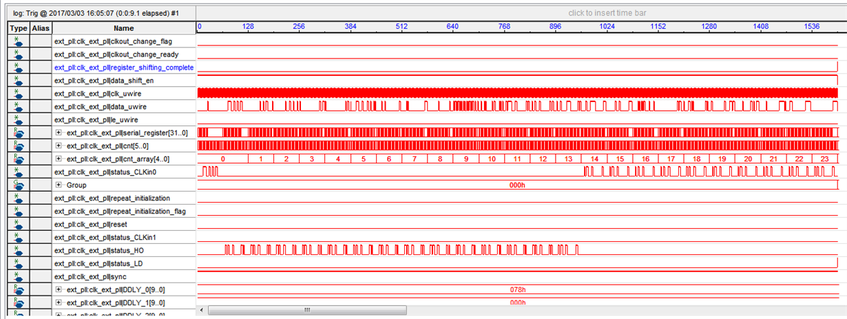
    We are suggesting you to use our .txt file with all the registers we program to the LMK04906 are numbered and discribed, so probably you wouldn't have to decode any data and just use our file and TI programming tool. We also attached *.png files, which are logic analyzer's data printscreens of our issue. Myabe firstly you can repeat our initialisation sequence using your hardware, and if you wouldn't reveal the problem then maybe we have something different during initialization stage and we need to find out what is it. We think that after the first initialization after power-up LMK04906 goes into such a state where it becomes sensitive to some clock or data changes on inputs, which appeared on them during second initialization (our schematic design consists of FPGA, Clock Generator and LMK04906, and we turn on a Clock Gen from FPGA. After FPGA's internal PLL gets locked, we start to configure LMK04906).    

    // during initialization first of all LMK04906 is being reset by programming the reset bit. It can be seen by difference between readback pins.  Default is status_HO and status_CLKin0 is the one after initialization.

    LMK04906_first_init_success - first time initialization after power-up.  

    LMK04906_second_init_unsuccess - second initialization without cold reset on LMK04906 (registers written from first initialization still there). LMK04906 didn't reset here.

    LMK04906_second_init_success_reset - after second initialization without cold reset on LMK04906 with hot reset on FPGA

    LMK04906_third_init_success_after_readback - third initialization without cold reset on LMK04906 and after readback operation PLL enters some new state in which it could be succesfully initialized. 

    LMK04906_initialization.txt
    --R0 (address(4..0) = "00000") - clk_out_0
    						register_array(0)(4 downto 0)		<= (others => '0'); -- address
    						register_array(0)(31)				<= '0';	-- clk_out_0 - power up
    						register_array(0)(30 downto 28)	<= (others => '0');	-- analog delay off
    						register_array(0)(27 downto 18)	<= std_logic_vector(to_unsigned(DDLY_0,10)); --(p.56) digital delay 120 VCO clk periods 0-522
    						register_array(0)(17)				<= '0';	-- reset turn off
    						register_array(0)(16) 				<= '1';	-- digital delay HS0 (Even) - ref to p.38(table 8)
    						register_array(0)(15 downto 5)	<= std_logic_vector(to_unsigned(140,11));	-- for clk_out_0 = 17.5MHz (ADC1) (VCO 2450/140) p.58
    						--R1 (address(4..0) = "00001") - clk_out_1
    						register_array(1)(4 downto 0)		<= std_logic_vector(to_unsigned(1,5)); -- address
    						register_array(1)(31) 				<= '0';	-- clk_out_1 - power up
    						register_array(1)(30 downto 28)	<= (others => '0');	-- analog delay off
    						register_array(1)(27 downto 18) 	<= std_logic_vector(to_unsigned(DDLY_1,10)); --(p.56) digital delay 120 VCO clk periods 0-522
    						register_array(1)(17) 				<= '0';	-- powerdown turn off
    						register_array(1)(16) 				<= '1';	-- digital delay HS1 - ref to p.38(table 8)
    						register_array(1)(15 downto 5)	<= std_logic_vector(to_unsigned(140,11));	-- for clk_out_1 = 17.5MHz (VCO 2450/140) p.58
    						--R2 (address(4..0) = "00010") - clk_out_2
    						register_array(2)(4 downto 0)		<= std_logic_vector(to_unsigned(2,5)); -- address
    						register_array(2)(31) 				<= '0';	-- clk_out_2 - power up because of SYNC_QUAL requirements p.63(Ethernet output clk)
    						register_array(2)(30 downto 28)	<= (others => '0');	-- analog delay off
    						register_array(2)(27 downto 18) 	<= std_logic_vector(to_unsigned(DDLY_2,10)); --(p.56) digital delay 120 VCO clk periods 0-522
    						register_array(2)(17) 				<= '0';	-- must be 0
    						register_array(2)(16) 				<= '1';	-- digital delay HS2 - ref to p.38(table 8)
    						register_array(2)(15 downto 5)	<= std_logic_vector(to_unsigned(98,11));	-- for clk_out_2 = 25 MHz (VCO 2450/98) p.58
    						--R3 (address(4..0) = "00011") - clk_out_3
    						register_array(3)(4 downto 0)		<= std_logic_vector(to_unsigned(3,5)); -- address
    						register_array(3)(31) 				<= '0';	-- clk_out_3 - power up
    						register_array(3)(30) 				<= '1';	-- OSCin source
    						register_array(3)(29 downto 28) 	<= (others => '0');	-- analog delay off
    						register_array(3)(27 downto 18) 	<= std_logic_vector(to_unsigned(DDLY_3,10)); --(p.56) digital delay 120 VCO clk periods 0-522
    						register_array(3)(17) 				<= '0';	-- must be 0
    						register_array(3)(16) 				<= '0';	-- digital delay HS3 (DIV Odd) - ref to p.39(table 8)
    						register_array(3)(15 downto 5)	<= std_logic_vector(to_unsigned(1,11));	-- for clk_out_3 = 100MHz (OSCin/1) p.58
    						--R4 (address(4..0) = "00100") - clk_out_4
    						register_array(4)(4 downto 0)		<= std_logic_vector(to_unsigned(4,5)); -- address
    						register_array(4)(31) 				<= '0';	-- clk_out_4 - power up
    						register_array(4)(30) 				<= '1';	-- OSCin source
    						register_array(4)(29 downto 28) 	<= (others => '0');	-- analog delay off
    						register_array(4)(27 downto 18) 	<= std_logic_vector(to_unsigned(DDLY_4,10)); --(p.56) digital delay 120 VCO clk periods 0-522
    						register_array(4)(17) 				<= '0';	-- must be 0
    						register_array(4)(16) 				<= '0';	-- digital delay HS4 (DIV Odd) - ref to p.38(table 8)
    						register_array(4)(15 downto 5)	<= std_logic_vector(to_unsigned(1,11));	-- for clk_out_4 = 100MHz (OSCin 100/1) p.58
    						--R5 (address(4..0) = "00101") - clk_out_5
    						register_array(5)(4 downto 0)		<= std_logic_vector(to_unsigned(5,5)); -- address
    						register_array(5)(31) 				<= '1';	-- clk_out_5 - power down
    						register_array(5)(30 downto 28) 	<= (others => '0');	-- analog delay off
    						register_array(5)(27 downto 18) 	<= std_logic_vector(to_unsigned(120,10)); --(p.56) digital delay 120 VCO clk periods 0-522
    						register_array(5)(17) 				<= '0';	-- must be 0
    						register_array(5)(16) 				<= '1';	-- digital delay HS5 - ref to p.38(table 8)
    						register_array(5)(15 downto 5)	<= std_logic_vector(to_unsigned(50,11));	-- for clk_out_5 (VCO/10) p.58
    						--R6 (address(4..0) = "00110")
    						register_array(6)(4 downto 0)		<= std_logic_vector(to_unsigned(6,5)); -- address
    						register_array(6)(31 downto 28)	<= (others => '0');	-- must be 0
    						register_array(6)(27 downto 24)	<= std_logic_vector(to_unsigned(1,4)); --(p.58) clk_out_1 type - LVDS
    						register_array(6)(23 downto 20)	<= std_logic_vector(to_unsigned(1,4)); --(p.58) clk_out_0 type - LVDS
    						register_array(6)(19 downto 16)	<= (others => '0');	-- must be 0
    						register_array(6)(15 downto 11)	<= (others => '0');	-- analog delay clk_out_1 = 500ps + no delay
    						register_array(6)(10)				<= '0';					-- must be 0
    						register_array(6)(9 downto 5) 	<= (others => '0');	-- analog delay clk_out_0 = 500ps + no delay
    						--R7 (address(4..0) = "00111")
    						register_array(7)(4 downto 0)		<= std_logic_vector(to_unsigned(7,5)); -- address
    						register_array(7)(31 downto 28)	<= (others => '0');	-- must be 0
    						register_array(7)(27 downto 24)	<= std_logic_vector(to_unsigned(2,4)); -- clk_out_3 type - LVPECL p.58
    						---change----------------
    						-- register_array(7)(23 downto 20)	<= std_logic_vector(to_unsigned(8,4));	-- clk_out_2 type - LVCMOS (Norm/Norm) p.58
    						register_array(7)(23 downto 20)	<= (others => '0'); -- clk_out_2 type - logic low
    						---change----------------
    						register_array(7)(19 downto 16)	<= (others => '0');	-- must be 0
    						register_array(7)(15 downto 11)	<= (others => '0');	-- analog delay clk_out_3 = 500ps + no delay
    						register_array(7)(10)				<= '0';					-- must be 0
    						register_array(7)(9 downto 5) 	<= (others => '0');	-- analog delay clk_out_2 = 500ps + no delay
    						--R8 (address(4..0) = "01000")
    						register_array(8)(4 downto 0)		<= std_logic_vector(to_unsigned(8,5)); -- address
    						register_array(8)(31 downto 28) 	<= (others => '0');	-- must be 0
    						register_array(8)(27 downto 24)	<= (others => '0');	-- clk_out_5 type - powerdown
    						register_array(8)(23 downto 20) 	<= (others => '0');	-- must be 0
    						register_array(8)(19 downto 16) 	<= std_logic_vector(to_unsigned(2,4)); --(p.58) clk_out_4 type - LVPECL
    						register_array(8)(15 downto 11) 	<= (others => '0');	-- analog delay clk_out_5 = 500ps + no delay
    						register_array(8)(10)				<= '0';					-- must be 0
    						register_array(8)(9 downto 5) 	<= (others => '0');	-- analog delay clk_out_4 = 500ps + no delay
    						--R9 (address(4..0) = "01001")
    						register_array(9)(4 downto 0)	<= std_logic_vector(to_unsigned(9,5)); -- address
    						register_array(9)(30)	<= '1';
    						register_array(9)(28)	<= '1';
    						register_array(9)(26)	<= '1';
    						register_array(9)(24)	<= '1';
    						register_array(9)(22)	<= '1';
    						register_array(9)(20)	<= '1';
    						register_array(9)(18)	<= '1';
    						register_array(9)(16)	<= '1';
    						register_array(9)(14)	<= '1';
    						register_array(9)(12)	<= '1';
    						register_array(9)(10)	<= '1';
    						register_array(9)(8)		<= '1';
    						register_array(9)(6)		<= '1';
    						--R10 (address(4..0) = "01010")
    						register_array(10)(4 downto 0)	<= std_logic_vector(to_unsigned(10,5)); -- address
    						register_array(10)(31 downto 28) <= std_logic_vector(to_unsigned(1,4)); -- must be 1
    						register_array(10)(27 downto 24) <= std_logic_vector(to_unsigned(1,4));	--(p.59) OSC_out type - LVDS
    						register_array(10)(23)				<= '0';	-- must be 0
    						register_array(10)(22)				<= '1';	-- OSC_out - enable (p.60)
    						register_array(10)(21)				<= '0';	-- must be 0
    						register_array(10)(20)				<= '0';	-- bypass divider OSC_out (p.60)
    						register_array(10)(19)				<= '0';	-- normal operation OSC_out (p.60)
    						register_array(10)(18 downto 16)	<= (others =>'0');	-- OSC_out divider = 8(but it was bypassed)
    						register_array(10)(15)				<= '0';	-- must be 0
    						register_array(10)(14)				<= '1';	-- must be 1
    						register_array(10)(13)				<= '0';	-- must be 0
    						register_array(10)(12)				<= '0';	-- no divide VCO (p.61)
    						register_array(10)(11)				<= '1';	-- must be 1 because of using dinamic digital delay
    						register_array(10)(10 downto 8)	<= (others =>'0');	-- VCO devider = 8(but it was bypassed)
    						--change---------------- qualifying clock - clk_out_1
    						register_array(10)(7 downto 5)	<= std_logic_vector(to_unsigned(1,3)); -- CLK_out_1 is selected as a reference output clock
    						--change----------------
    						
    						--R11 (address(4..0) = "01011")
    						register_array(11)(4 downto 0)	<= std_logic_vector(to_unsigned(11,5)); -- address
    						register_array(11)(31 downto 27) <= std_logic_vector(to_unsigned(6,5));	-- (p.62) Single PLL mode, internal VCO
    						register_array(11)(26)				<= '1';	-- SYNC - enable, required for dinamic d.d. (p.62)
    						register_array(11)(25)				<= '1';	-- clk_out_5 will not be synchronized (p.63)
    						register_array(11)(24)				<= '1';	-- clk_out_4 will not be synchronized (p.63)
    						register_array(11)(23)				<= '1';	-- clk_out_3 will not be synchronized (p.63)
    						register_array(11)(22)				<= '1';	-- clk_out_2 will not be synchronized (p.63)
    						--change----------------
    						register_array(11)(21)				<= '0';--'0';	-- clk_out_1 will be synchronized (p.63)
    						register_array(11)(20)				<= '0';--'0';	-- clk_out_0 will be synchronized (p.63)
    						--change----------------
    						register_array(11)(19 downto 18)	<= (others =>'0');	-- should be logic low (p.63)
    						register_array(11)(17)				<= '1';	-- sync_qual - qualification by selected reference clock (clk_out_3)
    						register_array(11)(16)				<= '1';	-- SYNC is active low
    						register_array(11)(15)				<= '0';	-- SYNC auto off - manual mode
    						register_array(11)(14 downto 12) <= std_logic_vector(to_unsigned(0,3));	-- SYNC IO pin type (input)
    						register_array(11)(11 downto 6)	<= (others =>'0');	-- must be 0
    						register_array(11)(5)				<= '0';	-- XTAL disabled (p.73)
    						--R12 (address(4..0) = "01100")
    						register_array(12)(4 downto 0)	<= std_logic_vector(to_unsigned(12,5)); -- address
    						register_array(12)(31 downto 27)	<= std_logic_vector(to_unsigned(2,5));	-- PLL2 DLD (digital lock detect selection for LD pin)
    						register_array(12)(26 downto 24)	<= std_logic_vector(to_unsigned(3,3));	-- status_LD - output type
    						register_array(12)(23)				<= '0';	-- turning off as we use SYNC_QUAL = 1
    						register_array(12)(22)				<= '0';	-- turning off as we use SYNC_QUAL = 1
    						register_array(12)(21 downto 20) <= (others => '0');	-- must be 0
    						register_array(12)(19 downto 18) <= "11";	-- must be ones
    						register_array(12)(17 downto 9)	<= (others => '0');	-- must be 0
    						register_array(12)(8)				<= '0';	-- disable DAC for PLL1 tuning voltage
    						register_array(12)(7 downto 6)	<= std_logic_vector(to_unsigned(1,2));	-- holdover disabled (p.67)
    						register_array(12)(5)				<= '1';	-- must be 1
    						--R13 (address(4..0) = "01101")
    						register_array(13)(4 downto 0)	<= std_logic_vector(to_unsigned(13,5)); -- address
    						register_array(13)(31 downto 27)	<= std_logic_vector(to_unsigned(4,5));	-- asserting status_HO pin as "holdover status"
    						register_array(13)(26 downto 24)	<= std_logic_vector(to_unsigned(3,3));	-- asserting status_HO pin as output
    						register_array(13)(23)				<= '0';	-- must be 0
    						register_array(13)(22 downto 20)	<= (others => '0');	-- status_CLKin1 - logic low
    						register_array(13)(19)				<= '0';	-- must be 0
    						register_array(13)(18 downto 16)	<= std_logic_vector(to_unsigned(3,3));	-- asserting status_CLKin0 as output push-pull
    						register_array(13)(15)				<= '1';	-- diables the holdover mode from being activated because of PLL1 (p.68)
    						register_array(13)(14 downto 12)	<= std_logic_vector(to_unsigned(6,3));	-- status_CLKin0 - uWire readback
    						register_array(13)(11 downto 9)	<= (others => '0');	-- Clkin_select - CLKin0
    						register_array(13)(8)				<= '0';	-- status_CLKin0/status_CLKin1 is "active high"
    						register_array(13)(7 downto 5)	<= (others => '0');	-- CLKin0|1|2 are disabled (p.70)
    						--R14 (address(4..0) = "01110")
    						register_array(14)(4 downto 0)	<= std_logic_vector(to_unsigned(14,5)); -- address
    						register_array(14)(31 downto 30)	<= (others => '0');	-- setting time before loss-of-signal asserts (1200 ns)
    						register_array(14)(29)				<= '0';	-- must be 0
    						register_array(14)(28)				<= '0';	-- disable LOS detect (because this is for CLKin that we don't use)
    						register_array(14)(27)				<= '0';	-- must be 0
    						register_array(14)(26 downto 24)	<= std_logic_vector(to_unsigned(3,3));	-- status_CLKin1 type - output push-pull
    						register_array(14)(23)				<= '0';	-- must be 0
    						register_array(14)(22 downto 20)	<= (others => '0');	--	asserting CLKin buffers to be "Bipolar" for LVDS (p.71)
    						register_array(14)(19 downto 14)	<= std_logic_vector(to_unsigned(63,6));	-- high threshold of the voltage at which "Holdover mode" is entered
    						register_array(14)(13 downto 12)	<= (others => '0');	-- must be 0
    						register_array(14)(11 downto 6)	<= (others => '0');	-- low threshold of the voltage at which "Holdover mode" is entered
    						register_array(14)(5)				<= '0';	-- disables entering holdover mode dependency on DAC Vtune
    						--R15 (address(4..0) = "01111")
    						register_array(15)(4 downto 0)	<= std_logic_vector(to_unsigned(15,5)); -- address
    						register_array(15)(31 downto 22)	<= (others => '0');	-- asserting DAC value to 3.2 mV if in manual mode (p.72)
    						register_array(15)(21)				<= '0';	-- must be 0
    						register_array(15)(20)				<= '1';	-- selection of the DAC manual mode
    						register_array(15)(19 downto 6)	<= std_logic_vector(to_unsigned(512,14));	-- clocks before holdover mode (but holdover mode was disabled)
    						register_array(15)(5)				<= '0';	-- force holdover - disable
    						--R16 (address(4..0) = "10000")
    						register_array(16)(4 downto 0)	<= std_logic_vector(to_unsigned(16,5)); -- address
    						register_array(16)(31 downto 30)	<= (others => '0');	--	confirm that XTAL lvl is 1.65 Vpp (XTAL was disabled in R11)
    						register_array(16)(24)				<= '1';	-- must be 1
    						register_array(16)(22)				<= '1';	-- must be 1
    						register_array(16)(20)				<= '1';	-- must be 1
    						register_array(16)(18)				<= '1';	-- must be 1
    						register_array(16)(16)				<= '1';	-- must be 1
    						register_array(16)(10)				<= '1';	-- must be 1
    						--R24 (address(4..0) = "11000")
    						register_array(17)(4 downto 0)	<= std_logic_vector(to_unsigned(24,5));	-- address
    						register_array(17)(31 downto 28)	<= std_logic_vector(to_unsigned(0,4));		-- PLL2_C4_LF capacity (p.73)
    						register_array(17)(27 downto 24)	<= std_logic_vector(to_unsigned(0,4));		-- PLL2_C3_LF capacity (p.74)
    						register_array(17)(23)				<= '0';	-- must be 0
    						register_array(17)(22 downto 20)	<= std_logic_vector(to_unsigned(0,3));		-- PLL2_R4_LF resistance
    						register_array(17)(19)				<= '0';	-- must be 0
    						register_array(17)(18 downto 16)	<= std_logic_vector(to_unsigned(0,3));		-- PLL2_R3_LF resistance
    						register_array(17)(15)				<= '0';	-- must be 0
    						register_array(17)(14 downto 12)	<= (others => '0');	-- PLL1_N digital delay - 0 ps
    						register_array(17)(11)				<= '0';	-- must be 0
    						register_array(17)(10 downto 8)	<= (others => '0');	-- PLL1_R digital delay - 0 ps
    						register_array(17)(7 downto 6)	<= std_logic_vector(to_unsigned(3,2));	-- window size used for digital lock detect for PLL1 (p.76) 40ns - same as reset value
    						register_array(17)(5)				<= '0';	-- must be 0
    						--R26 (address(4..0) = "11010")
    						register_array(18)(4 downto 0)	<= std_logic_vector(to_unsigned(26,5));	-- address
    						register_array(18)(31 downto 30)	<= std_logic_vector(to_unsigned(2,2));		-- window size DLD must be 2
    						register_array(18)(29)				<= '0';	-- reference frecuency doubler bypassed (f_OSCin * 1)
    						register_array(18)(28)				<= '0';	-- internal VCO requires the negative charge pump polarity to be selected (p.77)
    						register_array(18)(27 downto 26)	<= (others => '0');	-- never mind as we are selecting TRI-STATE at PLL2_CP_gain
    						register_array(18)(25 downto 23)	<= (others => '1');	-- must be 1
    						register_array(18)(22)				<= '0';	-- must be 0
    						register_array(18)(21)				<= '1';	-- must be 1
    						register_array(18)(20)				<= '0';	-- must be 0
    						register_array(18)(19 downto 6)	<= std_logic_vector(to_unsigned(8192,14));	-- Number of PDF cycles which phase error must be within DLD window before LD state is asserted (p.78)
    						register_array(18)(5)				<= '0';	-- Enabling PLL2_CP (loop filter)
    						--R27 (address(4..0) = "11011")
    						register_array(19)(4 downto 0)	<= std_logic_vector(to_unsigned(27,5));	-- address
    						register_array(19)(31 downto 29)	<= (others => '0');	-- must be 0
    						register_array(19)(28)				<= '1';	-- Many VCXOs use positive slope (p.78)
    						register_array(19)(27 downto 26)	<= (others => '0');	-- never mind as we are selecting TRI-STATE at PLL1_CP_gain
    						register_array(19)(25 downto 20)	<= (others => '0');	-- pre divider CLKinX = 1
    						register_array(19)(19 downto 6)	<= std_logic_vector(to_unsigned(96,14));	-- PLL1 divider (p.79)
    						register_array(19)(5)				<= '1';	-- Entering TRI-STATE at PLL1_CP (loop filter)
    						--R28 (address(4..0) = "11100")
    						register_array(20)(4 downto 0)	<= std_logic_vector(to_unsigned(28,5));	-- address
    						register_array(20)(31 downto 20)	<= std_logic_vector(to_unsigned(2,12));	-- PLL2_R = 2 - reference frecuency will be 50MHz (OSCin/2)
    						register_array(20)(19 downto 6)	<= std_logic_vector(to_unsigned(50,14));	-- PLL1 N devider
    						register_array(20)(5)				<= '0';	-- must be 0
    						--R29 (address(4..0) = "11101")
    						register_array(21)(4 downto 0)	<= std_logic_vector(to_unsigned(29,5));	-- address
    						register_array(21)(31 downto 27)	<= (others => '0');	-- must be 0
    						register_array(21)(26 downto 24)	<= "001";	-- OSCin freq >63 to 127 MHz (100MHz)
    						register_array(21)(23)				<= '0';	-- phase detector frecuency <= 100MHz
    						register_array(21)(22 downto 5)	<= std_logic_vector(to_unsigned(7,18));	-- PLL2_N_cal = PLL2_N = 7 (to reach PDF = 50MHz)
    						--R30 (address(4..0) = "11110")
    						register_array(22)(4 downto 0)	<= std_logic_vector(to_unsigned(30,5));	-- address
    						register_array(22)(31 downto 27)	<= (others => '0');	-- must be 0
    						register_array(22)(26 downto 24)	<= std_logic_vector(to_unsigned(7,3));	-- PLL2_P (prescale divider) = 7
    						register_array(22)(23)				<= '0';	-- must be 0
    						register_array(22)(22 downto 5)	<= std_logic_vector(to_unsigned(7,18));	-- PLL2_N = PLL2_N_cal = 7 (to reach PDF = 50MHz)
    						--R31 (address(4..0) = "11111")
    						register_array(23)(4 downto 0)	<= std_logic_vector(to_unsigned(31,5));	-- address
    						register_array(23)(31 downto 22)	<= (others => '0');	-- must be 0
    						register_array(23)(21)				<= '0';	-- LEuWire must be low for readback
    						register_array(23)(20 downto 16) <= std_logic_vector(to_unsigned(readback_addr,5));
    						register_array(23)(15 downto 6)	<= (others => '0');	-- must be 0
    						register_array(23)(5)				<= uWire_lock;	-- 1: R0-R30 locked| 0: R0-R30 unlocked
    						

    Best regards,

    Ivan

  • Hi Timothy!

    Have you reviewed our *.png - files?

    Best regards,

    Ivan

  • I'm afraid I've not been able to make further progress at this time. Have you been able to continue some debug?

    73,
    Timothy
  • Hello Timothy!

    We haven't get any success with debug right now, nothing changes.

    Do you have some thoughts what we should do?