This thread has been locked.

If you have a related question, please click the "Ask a related question" button in the top right corner. The newly created question will be automatically linked to this question.

CDCM9102: Output clock not generating

Part Number: CDCM9102

Hi Team,

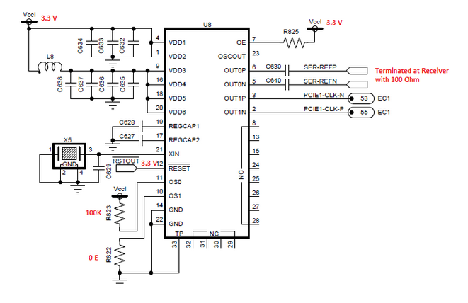
CDCM9102 device is being used at my customer in an application for 100 MHz clock generation (from 25 MHz crystal) . However, we are not observing any output. The other output is not terminated with 100 Ohm. Will this create any issue on the other output? 

Please find below the schematic section. Kindly request your suggestion to resolve the issue. Thanks.

Best Regards,

Suhas R C

  • Hi Suhas,
    I suspect XTAL didn't oscillate.
    Could you check X5 spec. C_load and C629 value? Notice there is a 8 pF Cin on pin Xin (inside of CDCM9102).

    Best Regards,
    Shawn

  • Try to reset again.
    Notice there are some words about reset pin.
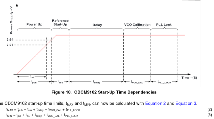
    "To ensure proper device operation, the oscillator must be stable before the low-noise clock generator
    calibration procedure. Quartz-based oscillators can take up to 2 ms to stabilize; therefore, TI recommends that
    the application ensure that the RESET pin is de-asserted at least 5 ms after the power supply has finished
    ramping. This can be accomplished by controlling the RESET pin directly, or by applying a 47-nF capacitor to
    ground on the RESET pin (this provides a delay because the RESET pin includes a 150-kΩ pullup resistor."
  • Hi Shawn,

    Thanks for your quick response. We probed XTAL and we are observing 25 MHz oscillations. C629 is not populated. Please find below the link to datasheet of the crystal. (ECS-250-10-36Q-ES-TR)

    https://www.ecsxtal.com/store/pdf/ECX-2236.pdf

    Best Regards,

    Suhas R C

  • Thanks for this suggestion. We will try it. Let us know in case we are missing any other point. Appreciate your help!

    Best Regards,
    Suhas R C
  • Hi Shawn,

    We tried applying reset to the device. However, we are still not able to obtain the output clock. 

    Kindly request your suggestion if there is something else that could be causing the issue.

    Thanks!

    Best Regards,

    Suhas R C

  • Hi Shawn,

    Any suggestions?

    Best Regards,

    Suhas R C

  • Hi Suhas,


    Could you measure each pin bias voltage?

    Pull-up resistor R823 = 100kOhm may be reduced to 10kOhm.


    Regards,

    Shawn
  • Hi Shawn,

    We have tested for the startup conditions. Captured the following waveforms. At startup sufficient time is available between power ramp up and RSTOUT deassert.  Please look at the waveforms and suggest any solutions.

    1. Power Rampup

    2. Blue one is Power and Yellow is RSTOUT

    3. Analog Node(VDD3,VDD4,VVD5, VDD6) and IO Node(VDD1, VDD2). All are applied simultaneously.

    We are meeting the following still Differential Clock Not generating.

  • How about pin OS0 and OE ?
  • Hi,

    We are getting 3.3 V on OS0 and OE. We also tested with reducing 100K to 10K on OS0. There is no differential output. It is unfortunate after sharing all the waveforms, BOM and schematic also we are not getting the responses. with this kind of support we will not go for TI parts in our new designs.

    Thanks & Regards,
    N.V.Subbaiah.
  • Hi N.V.Subbaiah,

    I am just back to work. Thank you for your details measurements.

    We could debug this chip by 3 part, as below figure.

    Pin OE could be floated or external pull-up to VDD, to enable outputs.

    1, Verify Block 1: OS1 (Pin 10), OS0 (Pin 11):1,1 LVPECL, OSCOUT = ON.

    When we get correct OSCOUT, Block 1 is good.

    2, Reset Block 2: RESET (Pin 12) : 0 → 1, Clock generator calibration

    We can't tell if Block 2 had worked normally or not, but could use reset to trigger it again when reference is ready.

    3, Verify Block 3: OS1 (Pin 10), OS0 (Pin 11):0,0 LVCMOS, OSCOUT = OFF

    LVCMOS driver is less affected by load than LVDS and LVPECL, high swing could be detected easily.

    If above 3 steps can't solve your problem, I have to guess this unit is broken (ESD issue or some else).

    Is this phenomenon on one board or on all boads?

    Hope this helpful.

    Best Regards,

    Shawn Han

  • Hi Shawn,

    We have tested both the cases with pull up and without pull up on OE. There is no output clock.

    1, Verified Block 1: OS1 (Pin 10), OS0 (Pin 11):1,1 LVPECL, OSCOUT = ON.

    we got correct OSCOUT,  25MHz clock. Block 1 is good.

    2, Reset Block 2: RESET (Pin 12) : 0 → 1, Clock generator calibration

    Used reset to trigger it again when reference is ready. There is no output clock.


    3, Verify Block 3: OS1 (Pin 10), OS0 (Pin 11):0,0 LVCMOS, OSCOUT = OFF

    There is no output clock.


    This phenomenon is there on all boards.

    We have replaced the CDCM9102 with the samples from another batch also.


    Thanks & Regards,

    N.V.Subbaiah


  • Hi N.V.Subbaiah,

    It seems something did not work.

    1, Make sure there are 10uF capacitors for pin 17 and pin 19. Measure voltage and compare them with EVM.

    2, Measure supply current for CDCM9102 by different OS1, OS0 setting. refer to below core current and buffer current.

    From current value, we may find some clue.

    FAE could help apply an EVM and more analysis. Thanks.

    Best Regards,

    Shawn Han

  • Hi Shawn,

    The problem is with RSTOUT Voltage. It is coming as 1.3v earlier. Now we have changed the resistor divider combination. We are getting 1.8v. After this clocks are generating. Thank you for your valuable suggestions.

    Thanks & Regards,
    N.V.Subbaiah
  • Hi N.V.Subbaiah,
    Thank you for your effort to debug it. Earlier 1.3V on RSTOUT pin would make an unsuccessful reset in chip internal at the beginning, and is hard to return to normal status with reset again.

    CDCM9102 datasheet provides 2 methods to control reset pin, directly controlling or applying a capacitor.
    ". Quartz-based oscillators can take up to 2 ms to stabilize; therefore, TI recommends that
    the application ensure that the RESET pin is de-asserted at least 5 ms after the power supply has finished
    ramping. This can be accomplished by controlling the RESET pin directly, or by applying a 47-nF capacitor to
    ground on the RESET pin (this provides a delay because the RESET pin includes a 150-kΩ pullup resistor.
    "
    Good to know you had solved it. Thanks.

    Best Regards,
    Shawn Han