This thread has been locked.

If you have a related question, please click the "Ask a related question" button in the top right corner. The newly created question will be automatically linked to this question.

ADS5294EVM INTERFACE TO ALTERA FPGA

Other Parts Discussed in Thread: HSMC-ADC-BRIDGE, ADS5294, ADS5294EVM

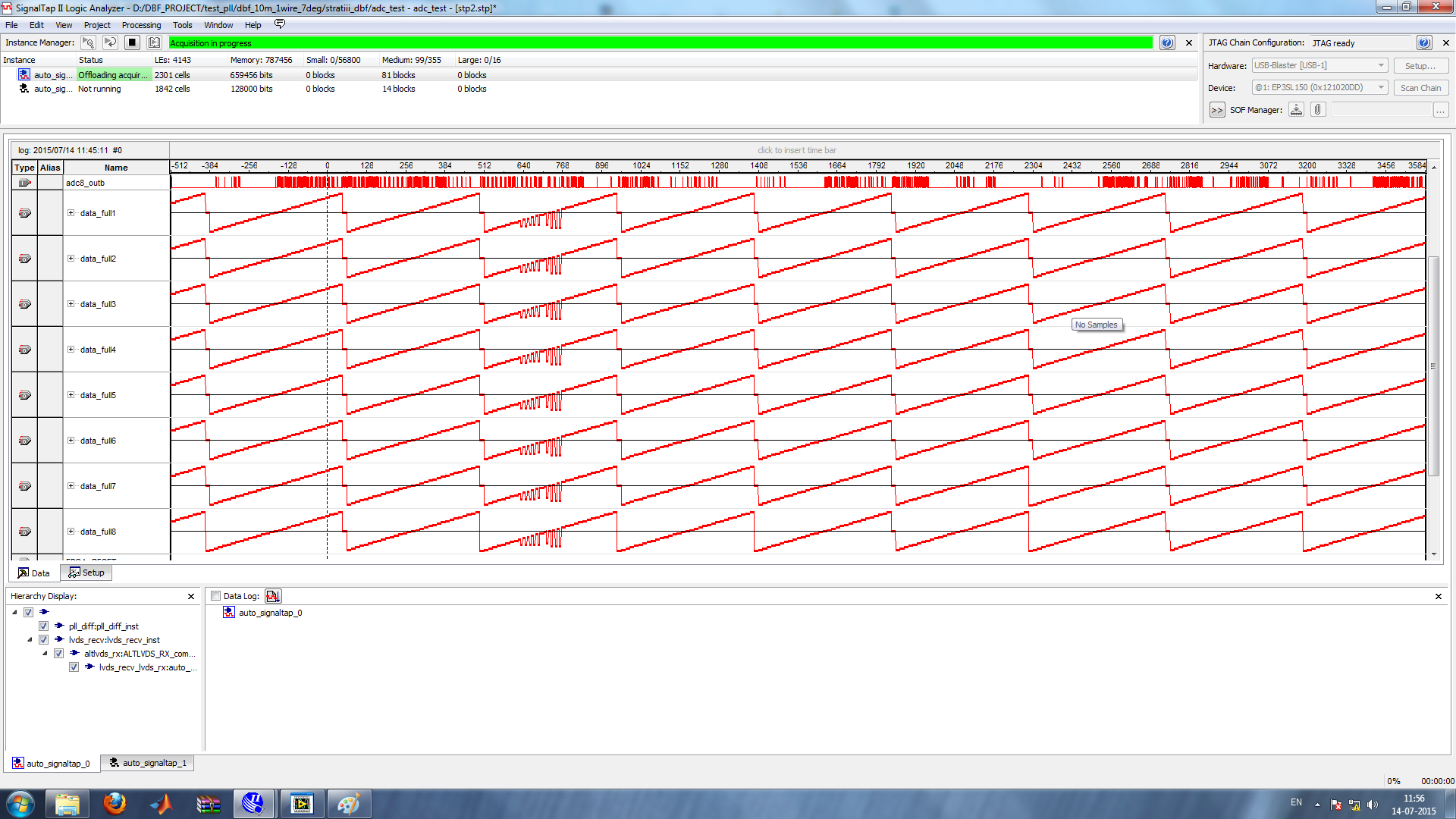
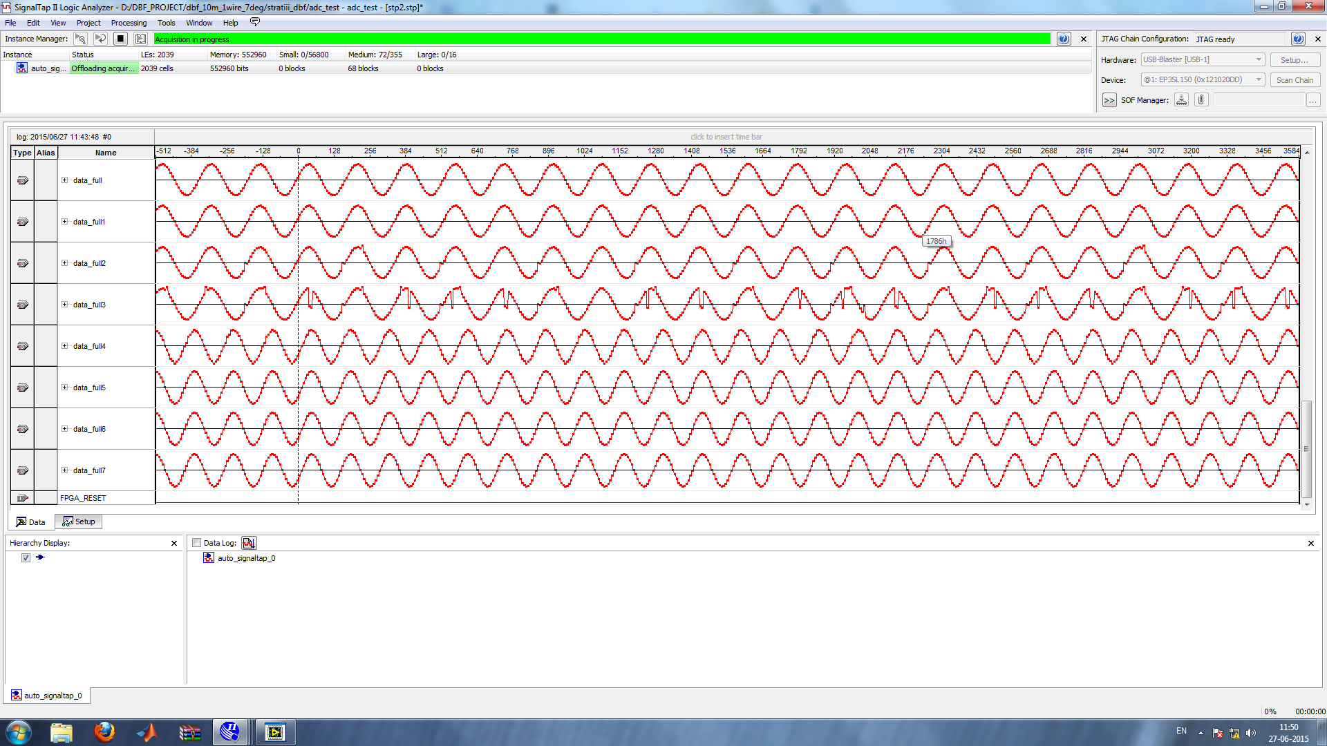
I need to interface ADS5294 EVM to ALTERA FPGA development board. I'm using Stratix III development board. With the help of HSMC-ADC-BRIDGE, i interfaced ADS5294EVM with STRATIX III board on HSMC port A. Whereas  i'm controlling ADS5294 EVM through USB with the help of GUI. So, if i test some test patterns susch as sync,deskew, ramp or custom pattern on adc channel outputs for a 2-wire interface (default setup on an ADS5294 EVM), channel b outputs are not at all toggling for few channels and at the same time, i'm not getting proper pattern. How to resolve the issue. What is the recommended guidelines to use EVM with FPGA board?


  • Manju,

    I'm assigning your post to the appropriate apps engineer.

  • Hi,

    The ADS5294 has only 8 test pattern generators, one for each ADC.  In one wire mode, the test patterns will be observed as expected on the 8 active LVDS outputs (the other 8 LVDS outputs (2nd-wire)  will be inactive).  A RAMP test pattern will increment 1 code for each subsequent sample from code 0 to max code.  However, if 2 -wire mode is invoked the output of one test pattern generator is divided between two LVDS outputs with half the sample on 1 LVDS output and the other half of the sample on the other 2nd LVDS output as illustrated in Figure 47 and 48 of the datasheet.  Therefore, the RAMP pattern observed will be odd.

    The same applies to other test patterns such as SYNC test pattern (11111110000000).  This test pattern in two wire mode would be observed as all one's on 1-wire and all zero's on the 2nd wire.

    So with this knowledge you can see if the test patterns captured in 2-wire mode are as expected or not.  Also, you can try to program the ADS5294 to 1-wire mode to see if you capture the 'expected' test patterns on half of the LVDS outputs. Just keep in mind that when doing this, the output interface speed should be maintained by reducing the sampling clock by a factor of 2.  I hope this helps.


    Regards,

    Christian

  • By the way,test patterns verified on both 1-wire interface and 2-wire interface. In case of 1-wire interface with different sampling rates(10 to 40 Msps), ramp pattern is observed only for shorter period, then it loses sync. Is it because of timing violations if then how to resolve the issue. i enabled sync with GUI. Any other timing constraints which i need to follow on the FPGA side. Currently i'm using frequency and phase delay constraints using pll inside FPGA.
  • Hi,

    How many ADS5294 devices are you attempting to synchronize or are you using only 1 device?  Also, are you using decimation and the digital filters?  If not, the  SYNC signal is not required to align channels within a single device; the outputs are inherently synchronized.  If you are attempting to synchronize channels from several devices and/or one device utilizing decimation, then the SYNC signal has setup and hold requirements outlined in Figure 54 of the datasheet.  Please ensure you are respecting this timing.


    Finally, please provide more detail as to what you mean when you say "the ramp pattern is observed only for shorter period, then it loses sync".  At a good sampling rate, is the ramp pattern captured correctly for all time?  I am not clear on what you are observing.

    Regards,

    Christian

  • Currently i'm using one device. I'm not using any decimation/digital filters. The current settings of the GUI are: 1-wire LVDS, 14bits and DDR phase as "10" default state. While observing the ramp pattern, the pattern repeats for sometime then some misbehavior for few interval and repeats again. Sometimes peaks are also observed on the pattern. But if i verify either sync or deskew pattern, its fine.
  • How ADS5294EVM gets interfaced to TSW1400/TSW3100? When i read the app note understanding serial LVDS capturing from TI. two approaches were mentioned:one using IDELAY and other using PLL with different phase delays. which one i have to follow. Do i need to do for all channels. Is it fine if i do only at the time of reset. Or dynamically it has to be adjusted. Since i'm using HSMC ADC bridge which doesn't provide any SPI control signals through HSMC interface, how can i verify with sync and deskew pattern adjustment. By the way, i'm having alternate plan to evaluate 8-channel ADC with FMC ADC bridge with the help of Xilinx FPGA. Will i get any firmware, app note or support from TI side?
  • Hi,

    [Question] Currently i'm using one device. I'm not using any decimation/digital filters. The current settings of the GUI are: 1-wire LVDS, 14bits and DDR phase as "10" default state. While observing the ramp pattern, the pattern repeats for sometime then some misbehavior for few interval and repeats again. Sometimes peaks are also observed on the pattern. But if i verify either sync or deskew pattern, its fine.

    [Response]  It is strange that you only see errors on the RAMP test pattern and not other test patterns.  Please confirm the sampling clock speed.  Can you slow this down and see if the RAMP capture happens without errors?

    [Question] How ADS5294EVM gets interfaced to TSW1400/TSW3100? When i read the app note understanding serial LVDS capturing from TI. two approaches were mentioned:one using IDELAY and other using PLL with different phase delays. which one i have to follow. Do i need to do for all channels. Is it fine if i do only at the time of reset. Or dynamically it has to be adjusted. Since i'm using HSMC ADC bridge which doesn't provide any SPI control signals through HSMC interface, how can i verify with sync and deskew pattern adjustment. By the way, i'm having alternate plan to evaluate 8-channel ADC with FMC ADC bridge with the help of Xilinx FPGA. Will i get any firmware, app note or support from TI side?

    [Response]  The firmware implementation on the TSW1400 uses neither the IDELAY or the PLL methods.  Since only one DUT will be tested at a time with the TSW1400, the data outputs are inherently synchronized with the frame clock and no alignment is required.  Therefore, the only alignment that is done at every capture is a frame clock alignment.  The frame clock is treated as a data output and bit shifted until all ones are followed by all zeroes.  More complex systems with multiple devices might require the use of more advanced techniques such as those described in the app note.  The app note you reference is FPGA agnostic.  In other words, the same techniques described in the paper can be used in most LVDS FPGA receivers including Xilinx FPGAs. 


    Regards,

    Christian

  • Ya, i did slow down the sampling clock speed and verified the RAMP without errors. But i want sample rate of 40MSPS(1/2 of sampling rate settings with the GUI).

    This works fine only for 10MSPS(1/8 of the sampling rate). What is limiting this factor? and at the same, when i try to feed the sine wave through waveform generator, the response is fine for lower amplitude levels (less than 75 mVpp). Please clarify this.

  • Herewith i've attached the ramp pattern and also sine wave observed on the signal tap logic analyser of Altera Quartus tool. (Observation is for 10MSPS).
  • Herewith i've attached the ramp pattern as well as sine wave observed on the Altera Signal tap logic analyzer (Quartus II) for 10 MSPS (1/8 of sampling rate of GUI)

  • Hi,

    You provided two RAMP waveforms, one of which contains many errors across the entire RAMP and another that only contains a single region of errors on only 1 of the RAMPs.  What is the difference in the setup between the two RAMPs?  What sampling clock source are you using to the ADC?  Can you verify that the clock jumpers on the EVM are correct as outlined in the User’s guide? Also, can you try using the 40MHz crystal oscillator that is installed on the EVM just to eliminate the sampling clock as causing the problem..  Figure 19 of the user's guide shows how to configure the jumpers on the EVM to use the clock source.   Finally, is the sampling clock 10MHz for all 3 of the plots you provided?

    Regards,

    Christian