This thread has been locked.

If you have a related question, please click the "Ask a related question" button in the top right corner. The newly created question will be automatically linked to this question.

ADC10D1500: Issue with Gain among channels

Part Number: ADC10D1500

We are facing issues with ADC10D1500CUIT. There are 2 ADCs on a single board which are used for Gain and Phase measurements. In the arrangement, ADC1 - ADC2 are synchronized using autosynch feature.

Each ADC receives two analog signals and a clock of 1350 MHz connected in 1:2 De-mux mode.

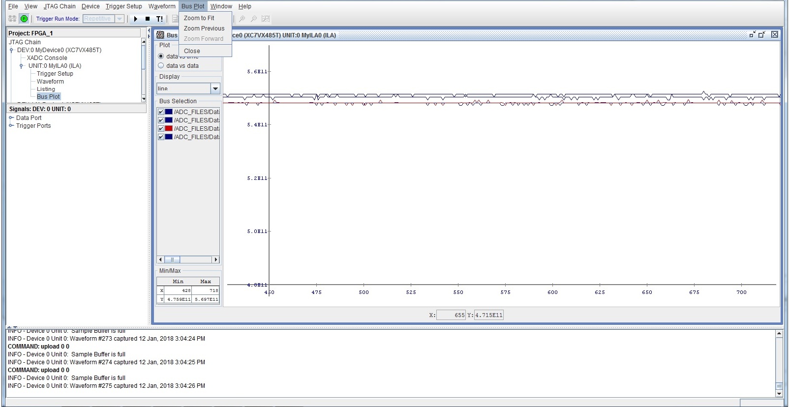
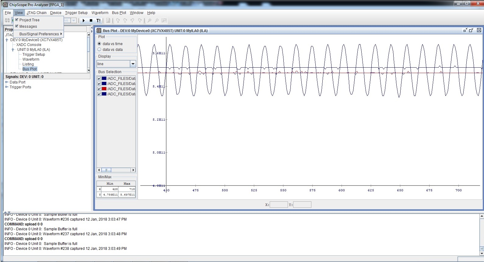
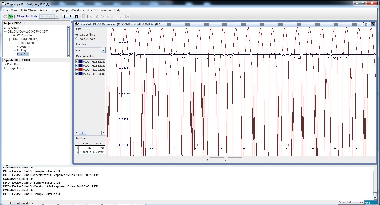
In some of the cards, we are facing issue with Signal Gain. We are applying the signal from same source to all channels of ADC’s (1GHz, 0 dBm to -40dBm).

In Higher Amplitude, Signal Level among all channels looks fine. But when signal level decrease, one of the channel (either ch-3 or ch-4) level shows higher level. Most of the time level will not decrease as per input below -16dBm. 

We have checked input circuits, Baluns, and Clock Circuits. They looks fine.

Register Setting of the ADC's are as below:

CONFIG_REG[0] <= 24'h400000;/
CONFIG_REG[1] <= 24'h422A00;
CONFIG_REG[2] <= 24'h440000;
CONFIG_REG[3] <= 24'h467FFF;
CONFIG_REG[4] <= 24'h48DA7F;
CONFIG_REG[5] <= 24'h4A0000;
CONFIG_REG[6] <= 24'h4C1C70;
CONFIG_REG[7] <= 24'h4E0000;
CONFIG_REG[8] <= 24'h500000;
CONFIG_REG[9] <= 24'h520000;
CONFIG_REG[10] <= 24'h540000;
CONFIG_REG[11] <= 24'h567FFF;
CONFIG_REG[12] <= 24'h580004;
CONFIG_REG[13] <= 24'h5A0000;
CONFIG_REG[14] <= 24'h5C0001;//e master


CONFIG_REG[0] <= 24'h400000;
CONFIG_REG[1] <= 24'h422A00;
CONFIG_REG[2] <= 24'h440000;
CONFIG_REG[3] <= 24'h467FFF;
CONFIG_REG[4] <= 24'h48DA7F;
CONFIG_REG[5] <= 24'h4A0000;
CONFIG_REG[6] <= 24'h4C1C70;
CONFIG_REG[7] <= 24'h4E0000;
CONFIG_REG[8] <= 24'h500000;
CONFIG_REG[9] <= 24'h520000;
CONFIG_REG[10] <= 24'h540000;
CONFIG_REG[11] <= 24'h567FFF;
CONFIG_REG[12] <= 24'h580004;
CONFIG_REG[13] <= 24'h5A0000;
CONFIG_REG[14] <= 24'h5C000F;//e slave

Please let us know what might be the reason for this mis-behaviour. How we can rectify this issue.

  • Hi Ramakrishna DC,

    We are looking into your issue, and will be back with you soon.

    Best Regards,

    Dan
  • Hi Ramakrishna

    Your register settings appear generally OK. I would recommend using a slightly lower Full Scale Range setting (Registers 3 and 11d (Bh)). Your current configuration is using the highest possible setting. This may interfere with proper device calibration, and doesn't leave any adjustment range to allow matching the full scale range of the multiple converters in your system.

    Can you confirm that after you write the listed register settings, you also perform an on-command calibration of the ADC using either the CAL input pin or CAL bit? Proper initiation of the calibration process can be observed by monitoring the CalRun output pin. Calibration must be performed after configuration, and with a stable clock and operating temperature. Calibration is required to optimize the Offset, Gain and Linearity of the ADC and achieve rated device performance.

    Can you share the schematic of the ADC and all related circuitry, including input signal path, clocking, power, etc?

    Best regards,

    Jim B

  • Hi Jim,

    Thank you for the replay...

    We have reduced the Full Scale Range setting to 790mV and tested.  I have also tried on command calibration of the ADC using CAL Pin. But there is no change in the result.

    I am attaching the schematic with this post. Please refer and suggest...ADC10D1500.pdf

    Thanks & Regards,

    Ramakrishna D C

  • Hi Ramakrishna

    I don't see anything obviously wrong in the schematics.

    When you test the ADC response with reduced input levels are you applying the same signal to all inputs simultaneously (ie. using a splitter) or is only a single ADC channel at a time tested?

    Can you terminate all other transformer inputs inputs and only apply the test signal to the balun transformer for the ADC channel being tested?

    If this is how you are testing I would expect the ADC to properly convert the input signal even as levels are reduced below -16dBm.

    If you have a strong signal on some channels and are only attenuating one at a time it is possible there could be coupling between the input paths and balun transformers between the strong signals and the attenuated channel being tested. If that is the case changing the placement of the transformers and routing of the input signal traces can help. If you would like me to review the placement and layout please send that information as well.

    Best regards,

    Jim B

  • Hi Jim,

    We are testing by applying same signals to all four channels. (Same frequency and signal strength.) . The signal source is a Signal Generator. This is applied to a 1:4 Power divider. Power divider is a calibrated one and has phase difference of 4 degree max. We have tested in below conditions:

    1) By Terminating all 4 channels:

    2) By applying signal to only 4th channel (Good one) and terminating all other channels.:

    3) Applying signal to only 3rd channel (the one which has issue) and terminating all other channels:

    I can see that the signal is not captured by the ADC correctly in 3rd channel. Input channel path is fine as we measured the input signal from spectrum analyzer just before Vin pin.

    --

    Thanks & Regards,

    Ramakrishna D C

  • Hi Ramakrishna

    The signal shown for the 3rd channel above looks like there is some issue with the data interface from the ADC LVDS outputs to the FPGA LVDS receivers. I have seen this type of signature in the past when there were issues with the DCLK to DATA timing in the FPGA capture logic, or the power supply voltages for the FPGA. The interface may work OK with the ADC test pattern but certain real world data patterns especially around mid-scale will tend to highlight the sensitivity of the data capture.

    Can you share the raw ADC data (binary or hex) for channel 4 and 3 show above?

    Best regards,

    Jim B