This thread has been locked.

If you have a related question, please click the "Ask a related question" button in the top right corner. The newly created question will be automatically linked to this question.

TSW30SH84EVM: TSW30SH84EVM PLL Settings

Part Number: TSW30SH84EVM
Other Parts Discussed in Thread: DAC34SH84, LMK04808

Hello,

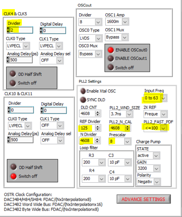
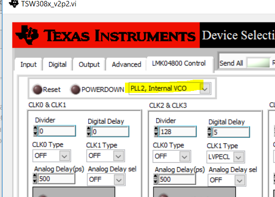
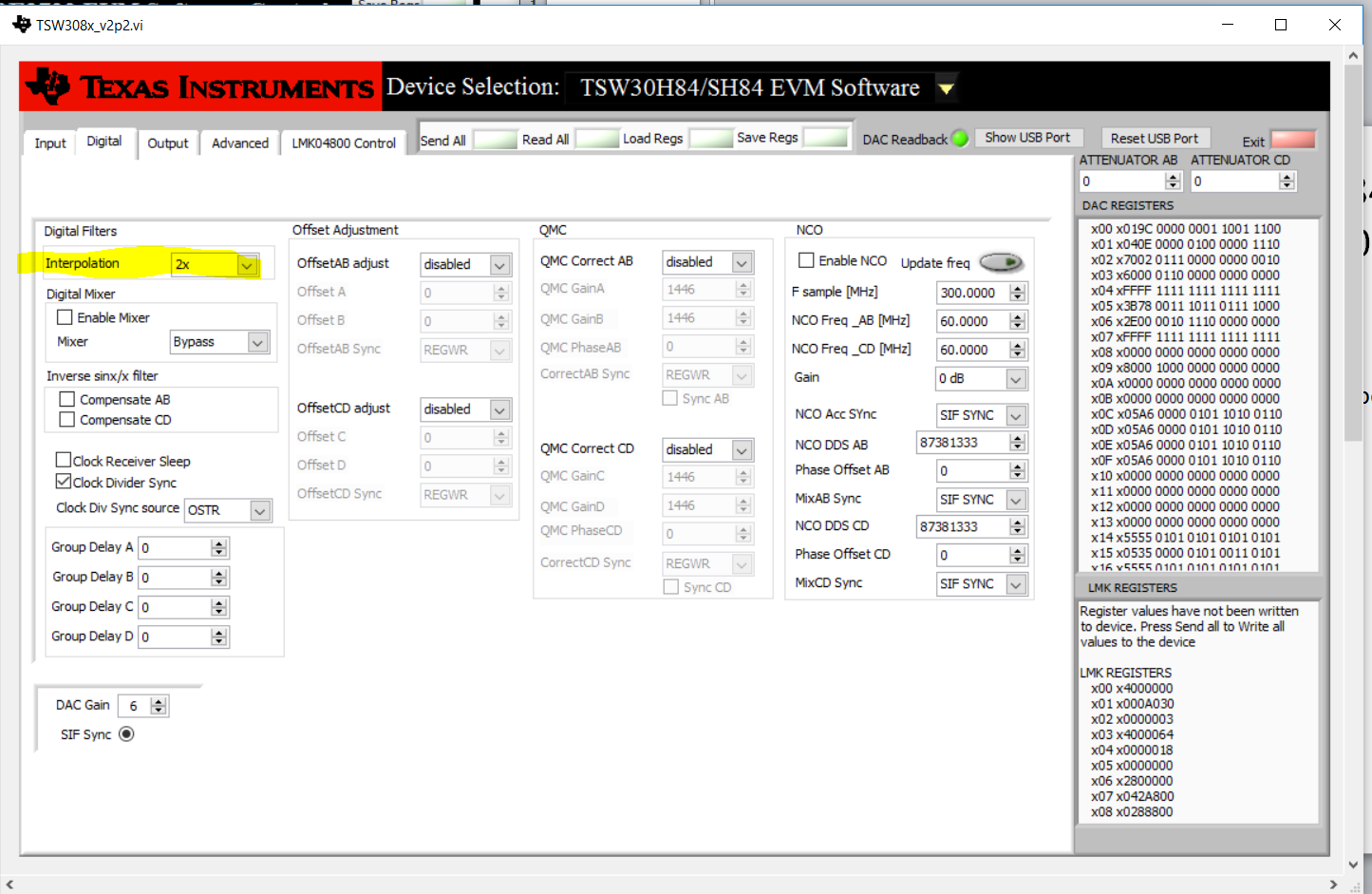
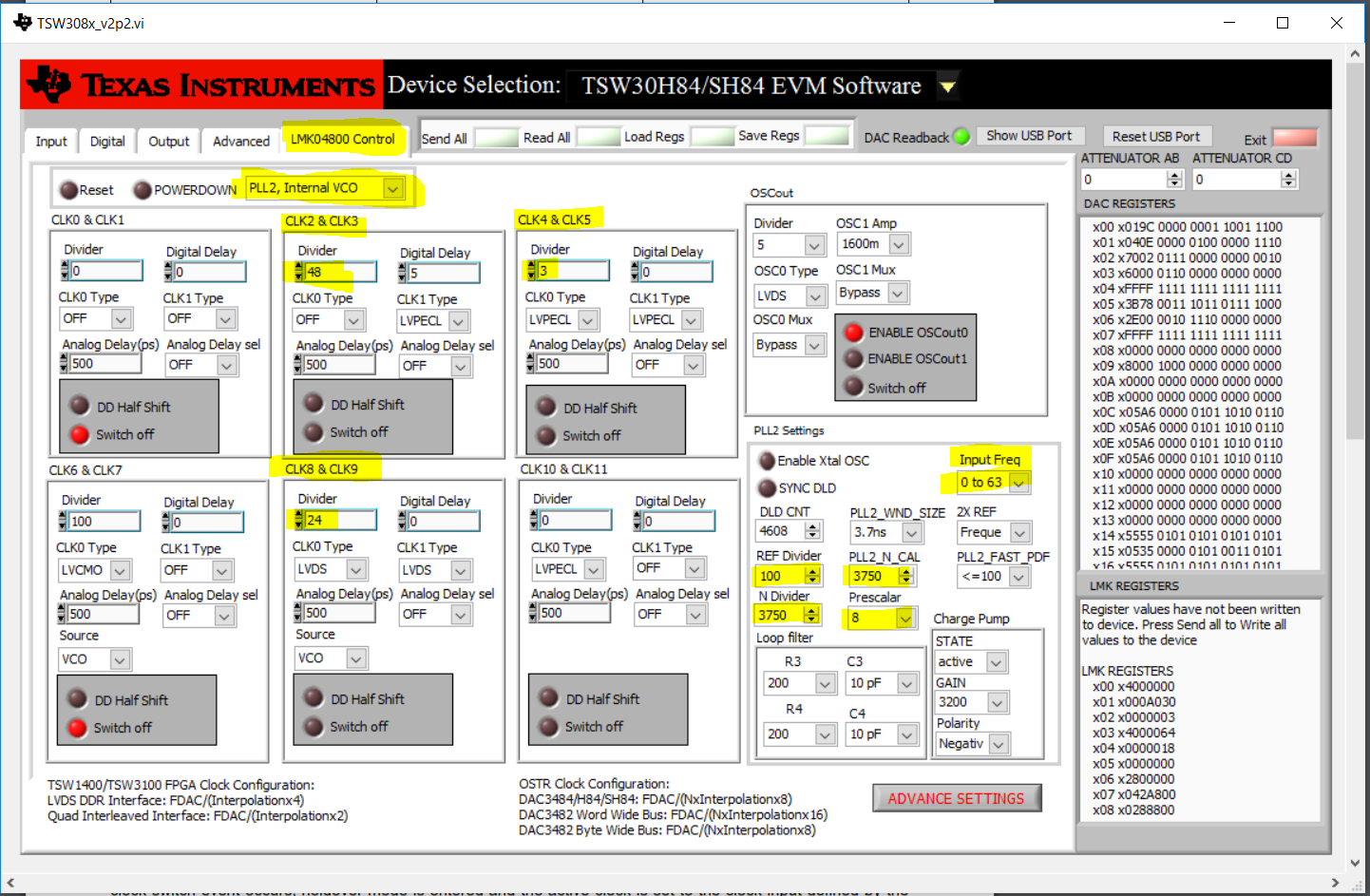
I am currently trying to use the PLL settings on the TSW30SH84EVM to control the DAC clock frequency and I am having issues following the example in the reference manual. I was wondering if there is anyway I could receive some guidance to using this setting in the TSW308x gui to control the DAC clock frequency and the data rate in the high speed data converter pro? Even if its just a configuration file that uses the PLL setting to set the DAC clock frequency that would be very helpful. I am also curious if I can use this PLL setting to set any data rate of my choosing to be used with the TSW1400EVM? 

Thanks, 

Joshua Johnson 

  • Hello Joshua,
    I have sent your question over to an engineer familiar with the DAC34SH84 (the DAC on the TSW30SH84EVM)
    Regards,
    Brian
  • Hey Josh,

    I will look into this when I get in the lab today and get back to you with an update before the day is over.

    Thanks

    Yusuf

  • Hey Josh,  

    There are a few different PLL modes available for clocking the DAC34SH84 when operating the TSW30SH84EVM. Adjusting Fdac depends on what mode you're using. Do you know what mode you are attempting to operate in?

    For the default mode the The TSW30SH84EVM  uses the single Loop mode of operation. This mode uses only one of LMK04808B;s PLLs (PLL2) and a reference frequency is provided by a 10MHz oscillator.

    For this mode, changing the DAC clock frequency requires calculating the following PLL2 divider values;

    R = Fref divider

    N = Feedback divider

    VCO N = VCO divider

    Prescaler.  

    I will walk you through an example. 

    If I want to adjust my PLL2 settings to output an Fdac of 1474.56M. First i need to find the VCO tuning range of my LMK device. For the LMK04808 the tuning range is 2750M to 3072M. Next I need to find a constant number ( VCO N), such that Fdac * VCO N = Fvco. Fvco is any frequency within the tuning range. 

    For a VCO N = 2, and an Fdac of 1474.56M, i derive an Fvco of 2949.12M. 

    Next i need to find the values for R, N, and Prescaler. The reference input frequency is set at 10Mhz and the desired PFD frequency is 80kHz. R divider needs to be set at 125 to satisfy the relationship PFD = Fref/R. 

    Next is to determine the prescaler divider. The prescaler divides the Fvco by its value and outputs the quotient to the N divider block. N is then determined by the PFD = (Fvco/prescaler)/N. 

    So with a Fvco of 2949.12MHz, a prescaler value of 8 and a PFD value of 80kHz. N is derived as 4608. 

    Here a snippet of the GUI with the calculated variables highlighted. The divider under CLK4 is the VCO N divider value. 

    Make sure to select the following option when entering the PLL register values. 

    Also, below is visual of the PLL2 with labels from the above example. I have also included an config file for the example we walked through.

    DAC34SH84_1474p58MHz_2xINT_NCO_0MHz_dual_sync_source_mode.txt
       x00	x019C
       x01	x040E
       x02	x7002
       x03	x5000
       x04	xFFFF
       x05	x3978
       x06	x3200
       x07	xFFFF
       x08	x0000
       x09	x8000
       x0A	x0000
       x0B	x0000
       x0C	x05A6
       x0D	x05A6
       x0E	x05A6
       x0F	x05A6
       x10	x0000
       x11	x0000
       x12	x0000
       x13	x0000
       x14	x0000
       x15	x4000
       x16	x0000
       x17	x4000
       x18	x280F
       x19	x0840
       x1A	x0020
       x1B	x0800
       x1C	x0000
       x1D	x0000
       x1E	x1111
       x1F	x8880
       x20	x2400
       x22	x1B1B
       x23	x07FF
       x24	x0000
       x25	x7A78
       x26	xB6B6
       x27	xEAEA
       x28	x4545
       x29	x1A1A
       x2A	x1616
       x2B	xAAAA
       x2C	xC6C6
       x2D	x0004
       x2E	x0000
       x2F	x0000
       x30	x0000
       x7F	x0000
    LMK REGISTERS
       x00	x4000000
       x01	x400A080
       x02	x0000002
       x03	x4000064
       x04	x0000010
       x05	x4000000
       x06	x2800000
       x07	x042A800
       x08	x0288800
       x0A	x48A0210
       x0B	x1BF8880
       x0C	x098600D
       x0D	x1D81033
       x0E	x0900000
       x0F	x4000400
       x10	x00AA820
       x18	x0000006
       x19	x0080800
       x1A	x47D2400
       x1B	x08000C1
       x1C	x03E8180
       x1D	x0001200
       x1E	x0001200
    ATTENUATOR AB
    0.00
    ATTENUATOR CD
    0.00

    Make sure the data rate is set  737.28M in the HSDC pro for the config file is using 2x interpolation. 

  • Hey Yusuf, 

    Thank you so much this is very helpful, but I have been trying this method that you are using to achieve 500 mbps on the high speed data converter (DAC frequency of 1000Mhz) and couldn't get a proper display on my spectrum analyzer. I don't have a specific method to use with the PLL I would just like to achieve any data rate of my choosing without using any external clock. This is a good method that makes sense to me but do you think you could walk me through an example on how to set a DAC frequency of 1000 Mhz, an interpolation of 2x, and a data rate of 500 mbps on the high speed data converter? 

    Thanks, 

    Joshua Johnson 

  • Sure no problem.

    Fdac = 1G

    Interp = x2

    Data rate = 500M 

    First lets do some math to figure out our divider values. 

    The VCO will only output frequencies within the range 2750M -3072M. The signal outputted by the VCO will need to be divided down by some number "VCO_div" to create our desired Fdac signal.

    I choose a VCO frequency(Fvco) of 3G. Now i need to find the following divider variables: VCO_DIV, Prescaler, N, & R. 

    To find VCO_DIV use the following logic.  Fdac = Fvco/ VCO_DIV;following this logic, VCO_DIV = 3. 

    next pick a prescaler value.This can be fairly arbitrary. The prescaler divides Fvco down by a constant value (2-8) and outputs the result to the N divider block. I picked a prescaler value of 8. So the signal leaving prescaler block and going to the N divider block is Fvco/8 = 375k. 

    Now pick a value for the R & N dividers. With a desired PFD of 100k, my N divider will be a value of 3750 and my R divider value will be 100k because the reference signal is provided internally by a 10MHz crystal. 

    Now determine what the divider values for the FPGA input 1&2(CLK8/9)  & OSTR(CLK2) clocks will be using the relationship noted in the user guide. 

    CLK8/9 divider value = VCO_DIV*Interpolation*4 = 24

    CLK2/3 divider value = VCO_DIV*interpolation*8 = 48

    Okay so now you have all of the values needed for your desired configuration. 

    Now, launch the GUI and load the config file i sent in the post earlier. We are going to verify or change the following settings. 

    First check and make sure that the PLL on the dac itself is disabled by going to the input tab. 

    Next make sure that under the digital tab, you set the correct interpolation which is x2 in this case.

    ....

    Next go to LMK control tab and make sure select the PLL2, Internal Vco option on the drop down tab. 

    Once you have done this you can enter all of the divider values we have already found. 

    Plug in the values we found earlier.

    Note that the "CLK4 & CLK5" Divider is VCO_DIV 

    Once you enter the appropriate values, click  the SEND ALL button towards the top of the page. You can verify that the PLL is locked by checking that LED D7 is lit. 

    Now open HSDC pro and select the correct device. set the data rate to 500MSPS. Generate a tone at 5MHz. and press send. 

    Connect the RF output SMA to  a spectrum analyzer and see what you get. 

    I am using a 1GHz LO so i expect to see a signal at 1005MHz. Which is what i get. 

    You can verify that the VCO is outputting 3G by connecting the spectrum analyzer to the CLKOUT3 SMA port (J2 or J3). 

    Hope this helps.