This thread has been locked.

If you have a related question, please click the "Ask a related question" button in the top right corner. The newly created question will be automatically linked to this question.

TPL0102-100: TPL0102-100RUCR Control issue

Part Number: TPL0102-100

Hi There

I had used TPL0102-100 as the current limit controller and my application is TOF camera. My schematic is below:

On the same PCB, I had SMT the old part before 2 years ago by sample from Avnet and can work fine. But recently, I buy new item from Mouser and it is not work after SMT on the same PCB. 

Below is parameter when module operation with Voxel viewer:

Voltage of RVar = 388mV

Voltage of WB pin in TPL0102:

    Work fine item: 130mV~188mV (can control by Illumination Power in Voxel viewer(100%~50%) )

    Work NG item: 193mV (can't control by Illumination Power in Voxel viewer )

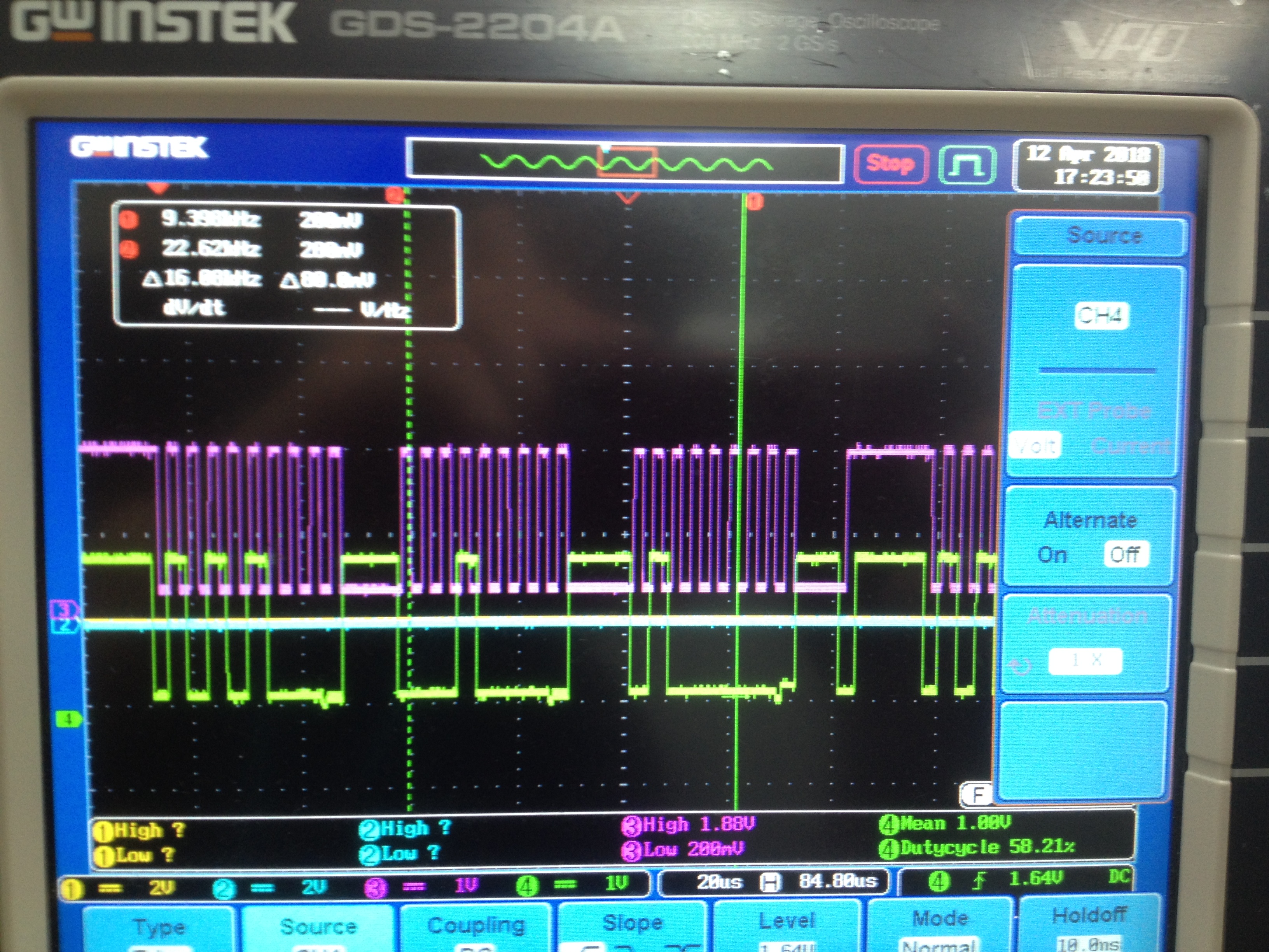
Below is scope capture the I2C pic, Red line=I2C_SLV_SCL_3V3, Green line=I2C_SLV_SDA_3V3:

Could you kindly give me support to clarify if the device defective?

Thanks.

Sincerely,

Nan

  • Hi Yen,

    Welcome to E2E and thank you for your query. I don't think the device is defective. This looks like a part-to-part variation within the accuracy of the device. You can try programming a code corresponding to the voltage output you are expecting.

    Hope that answers your question. Please let me know if you see any further issue.

    Regards,
    Uttam Sahu
    Applications Engineer, Precision DACs
  • I had program the same code to old and new device respectively. The old one can work fine, but the new one doesn't had any response.

    Thands for your reply.
    Nan
  • Hi Nan,

    Let me understand the problem properly - are you not able to change the resistance through programming? As I mentioned in my last post, could you please check it with another board or another device? This will help us quickly reach the root cause of the problem.

    Regards,
    Uttam
  • Hi Uttam

    Yes,I can't change the resistance through programming. I check for 5 pcs PCB with 5 pcs device from Mouser.And check another 5pcs sample request from TI website on 1 pcs PCB. All of these device are not response with the same program code.

    Thanks.
    Sincerely,
    Nan
  • Hi Nan,

    Sorry for the delay in replying due to my travel last week. I am analyzing the issue. Looking mainly into the programming sequence. I will get back on this by tomorrow.

    Thank you for your patience.

    Regards,
    Uttam
  • Hi Nan,

    As your explanation is pointing more towards unpredictability in the programming, I looked into the scope shot again and there seems to be some SDA edges transitioning during the clock transition. This might cause some setup/hold issue and different parts may have different response based on variability due to production. Could you please upload a scope shot with the SDA and SCL edges shown clearly? This will help us rule out the timing violations.

    Regards,
    Uttam
  • Hi Uttam

    Yesterday,I had used a I2C tool to program register address 0x01H, the Good and NG device just can work fine. So all the device is OK.

    So next, I check all I2C command from TOF host, and found some different between GOOD and NG device. First step, TOF Host will Read register address 0x0C and 0X0D, the Good device answered 0xAA, but the NG device answered 0x00. Second step, TOF host will program register 0x01 to change resistor value, the program code for Good device has 0x5A~0xE0 range by software setting, but for NG device it always be 0xFF. So that's why the resistor not be changed.

    Next I will ask out firmware member to check what the software will do if TOF host received wrong value from register address 0x0C and 0x0D. And check if we can cancelld the read step from host.

    Very thanks for your reply.

    Sincerely,

    Nan

  • Hi Uttam

    Here has some update with my test. I had test the I2C read function to get the value from register address 01h~10h.
    The reply from new device, only address 10h can read value 0x40 as 1 byte, in other address are more than 1 byte I get.
    The reply from old device,address 01h~0Dh and 10h can read as 1 byte, address 0Eh and 0Fh are more than 1 byte I get.

    I think because the read function has some error with new device, so the TOF module can't control the resistor correctly.
    I had check the I2C write function, and all device just work fine.

    please help to clarify this situation.
    Thank you very much.
    Best Regards
    Nan
  • Hi Nan,

    Could you please write down the steps you are performing in sequence? I think there are few values that are written in the non-volatile memory, which is different in your old and new device and the software you are testing now is ignorant of that. I don't see any device issue here in read or write mode. Please note that these are very old parts and each device goes through these tests during production. Hence, an interface functionality failure is the last thing we should doubt.

    Could you please share a scope shot of the read so that we can debug further? I think instead of comparing your old and new devices, you should check the function against the datasheet.

    Regards,
    Uttam
  • Hi Uttam

    My test step description is below:

    1. I use the I2C Sniffer tool to test I2C r/w function.

    2. As I power-on the device, first I read the register address 0x10h.

    3. Second I read the register address 0x00h.

    4. Finally I read the register address 0x01h, and there has error with NG device.

    Below picture is description of UI in I2C Sniffer:

    The measure message of my test show in picture as below:

    1. Good Device

    2. NG Device 01

     NG Device 02

    Command structure description: {S A8 10 S A9 P}

    S mean: Start bit

    P mean: Stop bit

    R mean: Read 1 byte

    Both address 10h in old and new device are reply same value 40h, but different in address 00h and 01h. Especially in address 01h with picture of NG Device 01, the reply does not contain stop bit, because the SDA would be hold low when command first send. When I resend command{S A8 01 P S A9 R P} five times, I finally got stop{P} bit, show in picture of NG Device 02.This statement is the same as read the register address 02h~0Fh. So as the TOF module will read register address 0x0Ch and 0x0Dh, because of not reply correctly, so I can't control the resistor value.

    Below is scope shot for NG device with I2C command {S A8 01 P S A9 R P} (Yellow line: i2c_clk, Green line: i2c_sda):

    1. First send

    2. Re-send 1

    3. Re-send 2

    4. Re-send 3

    5. Re-send 4

    6. Re-send 5

    Below is First command detail:(Yellow line: i2c_clk, Green line: i2c_sda)

    1. Start bit

    2. First byte(write address A8h)

    3. Second byte(write register address 01h)

    4. Stop bit and re-Start bit.

    5. Third byte(read address A9h)

    6. Fourth byte(read value 80h)

    7. SDA hold low

    Thanks

    Best Regards

    Nan

  • Hi Nan,

    In your waveforms, I see that there is a shift in the LOW voltage level on the SDA line. Is it inevitable? I suspect this might be causing the issue. I am not sure why this causes a problem with the READ and not the WRITE, but we can check what is the cause of this and is this meeting the VIH/VOH specs or not. Is it possible for you to check with a clean I2C source and see if the READ becomes proper or not?

    Regards,
    Uttam
  • Hi Nan,

    Do you have any update on this?

    Regards,
    Uttam
  • Hi Uttam

    Not yet, I will test it before Friday.

    Thanks a lot.

    Best Regards

    Nan

  • Sure. Thanks.

    Regards,
    Uttam
  • Hi Uttam

    The shift of LOW voltage is not observed with I2C tool only, as below picture:

    As the device spec as below:

    The VDD I used is  +3.3V, so the VIH=+2.31V and the VIL is 0.99V. In the scope the LOW voltage shift is not over 0.5V, so the I2C level is meet the spec. Below is picture of voltage shift with device:

    Thanks

    Best Regards

    Nan

  • Hi Nan,

    My apologies for delay in responding. When I look at your latest scope shots, in the first image you are getting a NACK and in the second one, you are getting an ACK. Could you please explain what is the difference between the two? I am not able to make out. Both of them look like WRITE sequences. Could you please capture some READ sequences?

    Regards,
    Uttam
  • Hi Uttam

    The first image is without slave device for I2C, and second image is with TPL0102 as I2C slave device. They are same I2C WRITE code, but I capture the first two bytes indicated what address I would like to READ.

    Below is the image captured READ sequences:

    Thanks

    Best Regards

    Nan

  • Hi Nan,

    Sorry again for replying so late - too busy weeks. The images indicate that the DPOT acknowledges the READ sequences but are you sure whether the I2C source is able to recognize the elevated VOL from the DPOT? May be a comparison with your working device may help.

    Regards,
    Uttam
  • Hi Uttam

    What is DPOT means?

    Below images are the scope captured for working device:

    COMMAN:Read the register 01h value, and return AAh. 

    Thanks.

    Best Regards,

    Nan

  • Hi Nan,

    If I compare the scope shots from working and non-working devices, I can see that the VOL of the SDA is higher for the non-working devices. Although it may be within the DAC spec, it may be on the border or out of range of your I2C source and hence, it may not be able to detect it. Is it possible to use another source or an I2C buffer in between?

    Please let me know in case you see any other difference between the scope shots I am not able to see.

    Regards,
    Uttam
  • Hi Uttam

    I think your concern is the red arrow in below image,right? (UP is working device, DOWN is non-working device)

    I think they are ACK from device and data return from device, so is it the issue for I2C tool ?

    Thanks

    Best Regards,

    Nan

  • Hi Nan,

    I understand your point. The fact that the SCL pulses after the ACK is being sent somewhere indicates that the controller is able to interpret the ACK. Please confirm whether there is setting for ignoring NACK's.

    However, in absence of any other strong lead, I would suggest testing with another controller so that we can reach closer to the root cause.

    Regards,
    Uttam