This thread has been locked.

If you have a related question, please click the "Ask a related question" button in the top right corner. The newly created question will be automatically linked to this question.

ADC128S102: ADC128S102

Part Number: ADC128S102

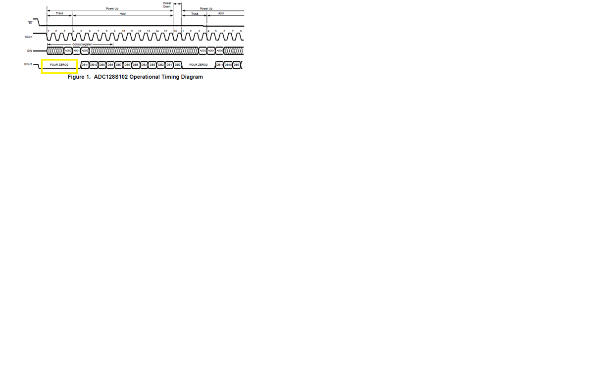
I am seeing something other than all zeros in first 4 bits of the "Data Out" serial data after the CS for the ADC128S102 is asserted.

Please see attached file which shows the timing from the data sheet.  I highlighted in yellow where the 4 bits should be zero.  The rest of the Data Out stream looks ok, i.e., the 12 bit ADC reading appears to be consistent with the voltage I presenting to the ADC.

I can provide more details, but I'm just hoping that someone has seen this before and recognizes the problem.

  • Hello,

    Is there a pattern or consistency to the first four bits? Are they always the same, or seem to depend on the input you use?

    It is good to hear that you are getting the correct conversion results. Are you using a known DC value to test this out?

    Would you share an oscilloscope shot of the digital communication, including SCLK, SDO, SDI, CS? 

    Regards, Cynthia

  • Hi Cynthia,

    Thanks for taking the time to reply.

    I am reworking the board now to add a 2200 pF cap from the ADC128S102's CH1 input to ground in order.  This of course is recommended for this switched capacitor ADC, I had failed to include it in the design.

    I have not had a chance to get a picture of the SPI comm but will shortly.

    However, I believe, and I would like to know what you think, that the problem is in the tracking since the ADC goes into Track mode for the first three SPI SCLK cycles after /CS is asserted.  My guess is that Track mode relies on that capacitor (that is not there) to absorb the kickback charge.

  • Hello,
    Would you point out where the 2200pF capacitor was recommended?
    The input componenets are usually designed for the input. Usually the input driving ciruit consists of an amplifier with an RC filter at the output, this is the input to the ADC.
    Every application of course has different needs, but all need to have the input settle within the aqsuition time of the ADC. Are you sure yout input can drive this capacitor at the CH1 input? If you would like, we can review your schematic.
    Regards
    Cynthia
  • Hi Kenneth!

    How is the ADC128S102 testing going? Have you resolved the issues?