This thread has been locked.

If you have a related question, please click the "Ask a related question" button in the top right corner. The newly created question will be automatically linked to this question.

ADS1282EVM-PDK: Anything in the EEPROM would prevent me from building a custom daughter board?

Part Number: ADS1282EVM-PDK
Other Parts Discussed in Thread: ADCPRO

I’m currently playing with an ADS1282EVM-PDK and I would like to design a new daughter board. I would use the same ADC, but changing the input stage and some PS and digital stuff details. This would be a prototype to validate a design concept for a future electronics, so that I handle the analog difficulties now while I let the digital design for a later stage.

I’ve a doubt. Checking the schematics I see there is an EEPROM in the ADS1282EVM-PDK (U14). If I build my own custom daughter board using the same memory with the same connections, would that work?

In other words, is there any information in the EEPROM, when the EVM is sold, that is critical?

Of course, do not hesitate letting me know if you feel I may find other difficulties while trying to make my new daughter board.

Thanks,

  • Hi Marti,

    Technically, no - the EEPROM on the ADS1282EVM-PDK just contains detail on the when the board was built and tested.  That being said, the ADCPro tool does read that EEPROM to try and ensure the correct EVM plug-in is loaded based on the hardware mounted to the MMB0.  You can try going into the INI file located at "C:\Program Files (x86)\ADCPro\plugins\evm\ADS1282\adcpro_evm.ini, and making sure that this configuration file has the text "EEPROMVerify=FALSE". 

  • Would there be any problem if I remove the EEPROM from my design?
  • Hi Martí,

    I don't think so, but if you want to be sure you can try removing the EEPROM from the ADS1282EVM and modifying the INI file, as Tom suggested.

  • Hello,
    Thank you very much for your answers. The inputs are very much appreciated. I tried removing the EEPROM on the ADS1282EVM-PDK and it didn’t work. I did as follows:
    1. Desolder lead 8 (power) of the EEPROM and bend upwards (disconnect)
    2. Test: ADCpro connects, downloads, stays for some time at “DSP not ready, retrying”, then error window “The firmware load has failed due to a timeout condition. Please reset the hardware to continue loading the firmware.” pops. The “number display led” on the MMBO is at “5”.
    3. Solder lead 8 (power) of the EEPROM back to the PCB.
    4. Test: Works fine. Boot is done and noise spectra are obtained with ADCpro
    5. Desolder leads 5, 6, 7 & 8 of the EEPROM (slightly lifting this side of the component)
    6. Test: same failure as step 2
    "EEPROMVerify=FALSE" was verified as Tom suggested. I didn’t change it as it was already FALSE and I kept it that way all the time. I didn’t try desoldering the other 4 leads of the EEPROM as I didn’t see the point. Any new ideas?
    Kind regards,
    Martí
  • Hi Marti,

    OK - we'll need to dig into the plug-in a little to try and understand what else might be going on there. Give us a few days to look into the code.
  • Sure Tom, I understand.

    Putting an empty EEPROM on my daughter board would also be a valid option, but not being able to remove the EEPROM from the original EVM makes me doubt about the feasibility of this option. It would be important for me to know for sure because it has an impact on my development plan.

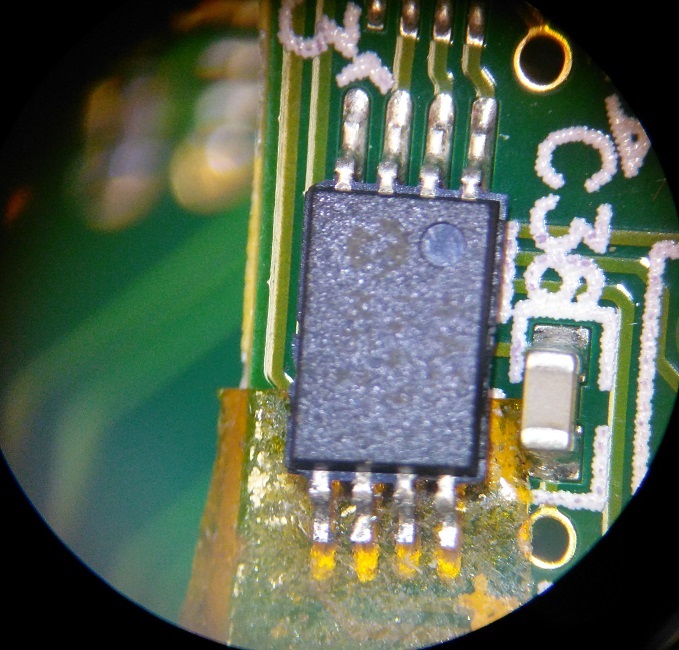
    Picture of the half removed EEPROM: my current status. If nothing is broken I should still be able to go back to the original configuration.

    Out of curiosity. My technical intuition and short experience with this kind of equipment makes me think that replacing a pluggable part of an evaluation module should be “common practice” by customer designers, in their way of learning the equipment better and anticipating development difficulties. Actually, when I bought the ADS1282EVM-PDK, I thought that one of the reasons it was split into two PCBs was so that the customer could build his own daughter board. (the other reason being that TI probably saves resources by using the same mother board with different EVM daughters, of course).

    Am I wrong?

    Looking deeper into the forums I just found two recent threads by Dean Gacita who seems to be facing the same problem at the moment. The issue seems open for him too.

    Is our development approach so uncommon? Don’t you have feedback from other customers trying to build their own daughter boards for the MMB0?

    Thank you very much for the time you are investing in this issue. Do not hesitate asking if anything in my posts is not clear, or if you need other information or tests from me.

    Have a nice day

  • Hi Martí,

    I can answer you latest question...

    Martí Bassas said:
    Is our development approach so uncommon? Don’t you have feedback from other customers trying to build their own daughter boards for the MMB0?

    I would say that is is more common today than it was 10 years ago when this EVM was released...
    The original intended use of the ADS1282EVM-PDK was to allow for quick evaluation of the ADC's performance, and hopefully if it met the application requirements, the customer would then begin their own hardware and software design using the form-factor they needed. To this end we provided the MMB0 and the ADCPro software to allow for this kind of evaluation, but the purpose of the EVM hardware and software most ended there as it want not intended to be a type of development platform.

    More and more, I do see the usefulness of rapid prototyping, using hardware that is more specific to customer end-applications, and so I think you will start to see more flexibility in future TI EVMs...
    In most cases I think customers will have much different hardware form-factors from the EVM, but perhaps it wouldn't be unreasonable to allow for some kind of header (test point) connection to the ADC (on the customer hardware), which could be connected back to the EVM motherboard and allow for evaluation of the customer's hardware with the same EVM software. If you have any additional comments or feedback regarding this idea or others involving the EVM I'd be more than happy to consider it for future EVMs. Thanks!


  • Hi Marti,

    We looked into the code and it seems like the ADS1282EVM plug-in was done a little differently and turning the EEPROM verify off ("EEPROMVerify=FALSE") is not going to work out on this board after all. I'd have to see if putting a blank EEPROM works, since the code is expecting to (at least) see something at that particular I2C address.

    I also wanted to expand a little on Chris's comments. The EVM's that were designed to accompany the MMB0 were in fact meant to be 'user friendly' from the standpoint of the male and female headers located on the boards. Yes - they plug into the MMB0 and use our ADCPro software, but there is no reason why you couldn't remove the controller and use your own processor to 'fly wire' your control signals into our EVM. We don't restrict you from gaining direct access to the ADC through your favorite MCU/DSP, etc. We've had quite a few people take that approach since our ADCPro Software a limiting factor in end product development. As Chris mentioned, we never intended the MMB0 to be used as a development platform. I'm sorry that I gave you bad information regarding the disabling of the EEPROM...
  • Hello Tom and Chris
    Buying a blank EEPROM and replacing it in the ADS1282EVM unit I have is something I would do if I need to. For me it is key to know if I can go on with my baseline development strategy or not. It would take me a few weeks as I will probably be busy with other projects and this one is not top priority schedule wise. Of course I would post the result on the thread. However, if you plan to test it yourselves anyway I will be happy to just wait and see. Is it the case?
    Concerning the discussion about EVM-PDK role in design development I understand your points. I am still a little bit surprised that there aren’t more designers trying to use the MMB0 to test their analog circuit, even if MMB0 was not intended for this purpose, but I guess it is just me. People may often assume that the difficulties are to be expected in the digital & sw side and, as far as digital is ok, the analog side of the circuit should just follow. It might be true, at least in some cases, I don’t judge. For me, when I see such a resolution and like -140dBfs* noise levels, I am so amazed it even works that I cannot help wanting to go step by step.
    Thank you for your fruitful and informative comments,
    Martí

    *(full scale amplitude signal is 0dB reference. Rough value, it depends on gain and filter bandwidth used)
  • Hi Martí,

    I ran some tests here and found that removing the EEPROM indeed caused the ADCPro Plugin to not connect. The interesting thing was the two EVMs I tested had blank EEPROMs. We think that the ADCPro software is simply looking for an ACK from the I2C EEPROM, therefore, a blank EEPROM would seem to be a requirement on any testboard that intendes to utilize the MMB0 and ADCPro. For compatibility, I would also recommend keeping the U7 GPIO expander on your testboard.

    I'm not sure why this was implemented in this way, but this seems to be a quirk with this particular EVM that was later fixed with other ADCPro-based EVMs.

    I think the idea of reusing the EVM motherboard and software to test out the analog performance on a custom prototype board is a great idea, and it is something I will keep in mind when working on future EVMs!
  • Hello Chris,

    After thinking about it and discussing with some colleges my current plan was the following:

    A plan: Fully desolder the original EEPROM (U7), solder it on a small test PCB and route some wires to connect it directly to the MMBO (or connect it to the J5 pins and somewhere equivalent on my future custom board). It would have felt like hacking the EVM a little bit.

    B plan: Solder a blank EEPROM on my custom PCB.

    C plan: Ask you for the data in the EEPROM, burn it to a blank unit and put it on my custom PCB. I saw in a thread mentioned above that this data was given to Dean Gacita, so I was confident this was a solid backup plan, although It would have meant some more work.

    In any case I would have left a footprint for the EEPROM on my PCB so that plans B and C were easily available.

    After your input plan B gets upgraded to A, and C becomes less and less likely.

    Keeping the I2C I/O expander (U7) for compatibility with the MMB0 was already foreseen. I’ll add some jumpers so that my custom analog PCB can be used with or without the expander. It will be useful in the future to develop the digital electronics without the expander constraint.

    I start feeling that this design is simple enough to expect it to work without major issues. We will see…

    Thank you very much for these exchanges.

    Martí

  • Hi Marti!

    I actually like Plan A. De-soldering the EEPROM and mounting it 'stand alone' to the MMB0 is actually not that bad of an idea. There are screw terminals on the MMB0 which you can use to wire in power and ground from the MMB0 to the EEPROM. You could flywire the I2C lines, which would certainly be an option so long as you maintained the I2C address. None of this would interfere with your customized board as you could pick up SCL and SDA from the MMB0 itself.
  • Hello Tom,

    Exactly, this was the idea.

    Footprints J9 and RA3 in the EVM unit I have are not populated, so leads A0, A1 and A2 are floating. I assumed keeping the "good address" would be as easy as not connecting the A0, A1 and A2 pins.

    The drawback of this plan is that I may break something with the soldering/desoldering. It's "one shot". The cabling and routing is also more fragile, tickier and arguably uglier than placing a blank EEPROM on a propper footprint on my custom board.

    Martí