This thread has been locked.

If you have a related question, please click the "Ask a related question" button in the top right corner. The newly created question will be automatically linked to this question.

DAC37J82EVM: Link establishment fails during ILA sequence

Part Number: DAC37J82EVM
Other Parts Discussed in Thread: DAC37J82, , LMK04828

Hello, I'm attempting to establish a link between the DAC37J82 and a transmitter in an FPGA

Setup details :

  • DAC37J82EVM board
  • Xilinx VCU118 Demo board
    • JESD204 v7.2.1 IP is instantiated

  • JESD204B subclass 1
  • LMFKS = 4, 2, 1, 30, 1
  • 1 GSPS sampling rate, 250 MHz core clock, 10 Gbps line rate

I've followed the setup steps on page 107 of the DAC37J82 datasheet and when I trigger SYSREF from the LMK04828 on the DAC EVM, I see that SYNCB line from the DAC toggles between asserted and deasserted indefinitely. I'm not quite sure why this is since the ILA sequence being output by the FPGA looks good as far as I can tell.While in this state, the DAC EVM GUI reports a lane configuration error for lanes 0 - 3.

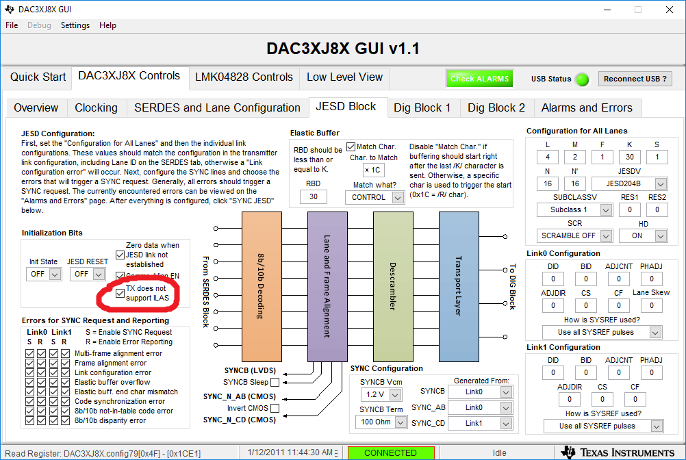
If I check the 'Tx does not support ILAs' box in the DAC EVM GUI, things seem to work a lot better. I can verify on a spectrum analyzer that my 374 MHz test tone generated in the FPGA is being properly output by the DAC.

Any help with figuring out why I the ILA sequence break the JESD link establishment would be greatly appreciated, thank you.

  • Hi Branden,

    One of our experts is reviewing your issue, and will be back with you soon.

    Best Regards,

    Dan
  • Thanks Dan. Here is the complete register configuration file for the EVM it helps

    DAC37J82EVM_setup.cfg

  • Branden,

    It appears you have an issue with the CGS stage. Have you checked the alarms that are reported in the "Alarms and Errors" tab of the GUI? In most cases I have seen, the LMK04828 output clock used by the FPGA has the wrong divider. The GUI settings are based on an Altera FPGA that we use on our pattern generator board. What I have noticed when using Xilinx boards, this reference clock is usually different by a factor of 2 from the Altera FPGA. See section 7.1 of the attached document for help with setting this divider properly.

    If this doesn't help, try your setup using K = 20 with a SYSREF frequency of 6.25MHz. This is what our GUI uses as a default when using your settings.

    Regards,

    Jim

     1258.KCU105 HSDC Pro User's Guide.pdf

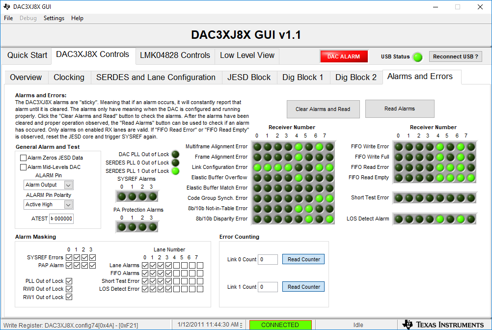
  • Thanks for your response Jim. Here is a screenshot of the alarms that are reported in the GUI :

    There is a link configuration error for lanes 0 - 3 (only when 'TX does not support ILAS' is unchecked) which is what led me to believe that the problem was during ILA. I am ignoring errors from lanes 4 - 7 since I have those disabled, is that OK?

    Regarding clocking, we are using 2.5 GHz as the internal VCO frequency in the LMK04828 that gets divided down by 10 to arrive at the 250 MHz core (and reference) clock for the FPGA. Xilinx documentation (PG066) states that the core clock rate must always be 1/40 the serial line rate. Fortunately, this agrees with Table 1 in the document attached in your post, allowing for a line rate multiplier of 40 for the REFCLK when the line rate is between 9.8 and 12.5 Gbps.

    I've also tried setting K to 20 and SYSREF to 6.25 MHz as you suggested but got the same link configuration errors as before.

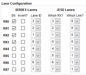
    One part of my configuration on the FPGA side that I had to correct was the lane ID mapping (e.g. physical lane 0 goes to JESD lane 3 on the DAC). I configured the lane IDs in the Xilinx JESD IP to match the following :

    This unfortunately did not solve my issue though. Are there any other lane configuration parameters that I could be missing?

    Thanks,

    -Branden

  • Branden,

    We have seen issues in the past when using Xilnix parts with serdes rate around 10Gbps. As a sanity check, can you try your setup with a serdes rate below 8 Gbps?

    What value are using for RBD? Just want to make sure this is equal to or less than your "K" value.

    Regards,

    Jim 

  • Hi Jim, I updated my settings so that the FPGA reference clock, core clock and DAC clock are all running at 125 MHz, bringing the serial line rate down to 5 Gbps.

    After making this change, I'm still seeing the same link configuration error alarms on lanes 0 - 3 reported by the DAC.

    My RBD value is currently 30, equal to my K value (It was set to 20 when I tested the setup with K = 20).

    I appreciate your help so far and am willing to try any other steps you can think of to debug this problem. In the mean time I'll let you know if I have any breakthroughs on my end.

    Thanks,

    -Branden

  • Branden,

    Can you send screen shots of every tab of the DAC GUI, including the LMK ones? I will see if something stands out. This is much faster than going through every register setting from the configuration file.

    Regards,

    Jim 

  • Sure thing Jim, here you go :

    dac_gui_all_tabs.zip

  • Branden,

    I went over your configuration file and I saw many things that I did not like. To keep things simple, can you run with an external clock source of 500MHz connected to J17 of the DAC EVM, and use the GUI settings from the quick start tab? I do not want to use the DAC PLL or any other features (NCO, mixer, ect...). I would like to focus on getting the link up and running with the easiest setup to start with. If you use the GUI settings, make sure you are using lane ID 0-3 from the FPGA. These are FMC pins C2/C3, A22/A23, A26/A27. and A30/A31. The only thing you might have to change is the LMK CLKOUT 0 divider. Also, make sure all JESD parameters used by the DAC are set the same in the FPGA. Do not load the FPGA firmware until the LMK has been configured properly.

    Regards,

    Jim

  • DAC37J82_421_DAC_PLL_setup.pptxDAC37J82_421_DAC_PLL_setup.cfgBranden,

    I got your setup running using the DAC pll with an external 125MHz reference clock going to SMA J17 on the DAC EVM (see attached files). If you need config files for a different reference frequency, let me know.

    Regards,

    Jim

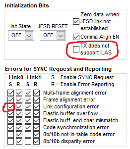
  • Hi Jim, I went ahead and configured the EVM using the quick start tab with a 500 MHz clock piped into J17 from a sig gen, making sure to configure the FPGA JESD IP correctly after the EVM was fully configured. I found that link establishment did complete successfully, so I started changing DAC and LMK settings to match my desired configuration one by one in order to find out where things break. Starting with the quick start configuration and making only the following changes, I observe identical behavior in terms of JESD link establishment as my desired configuration :

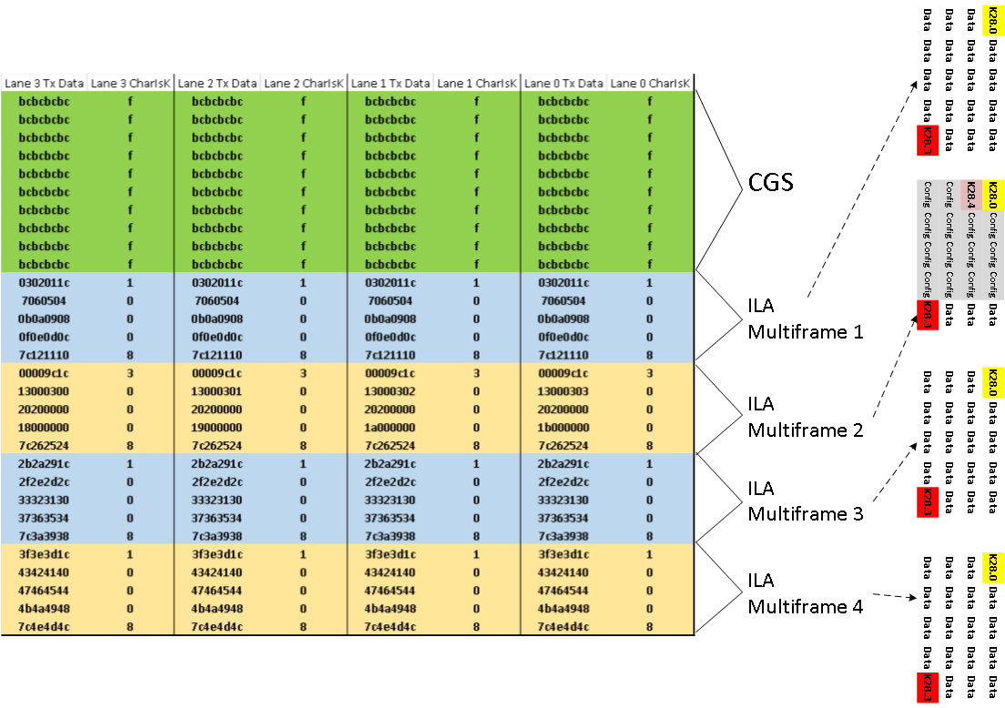
    With "Tx does not support ILAs" unchecked and SYNC request on link configuration errors enabled, I cannot establish a link with the FPGA. If I'm understanding this correctly, when not configured as in the image above, the DAC will ignore any errors during the CGS / ILA phases of link establishment? If so, I'm struggling to find errors in the ILA sequence from the FPGA that would prevent link establishment. Here is a diagram of the ILA sequence that I dumped from output of the JESD IP in Vivado :

    Referencing page 16 of this document, the structure of the ILA seems to be correct : www.ti.com/.../slap159.pdf

    I unfortunately don't have a copy of the official JESD204 spec on hand so I can't verify the config data is correct, but on quick inspection I can pick out what looks like the lane IDs and number of frames per multiframe.

    Are you able to replicate this behavior in hardware on your end?

    Thank you,

    -Branden

  • Good news!

    I was able to successfully establish a JESD link between the DAC and FPGA without the DAC ignoring the ILA today.

    The key was closely inspecting the link configuration data in the second multiframe of the ILA. I was able to find the details of the link configuration data spelled out on page 4-6 of UG-01142. It turns out there were a few important parameters that weren't being set, namely N, N' and HD. These cannot be set by default during IP generation in vivado so I made sure to manually set them via AXI after loading the FPGA bitstream.

    Part of the confusion also came from the lane reassignment needed for this EVM. I was originally reversing the order of the lanes (lane 0 --> lane ID 3, lane 1 --> lane ID 2, etc.) on both the FPGA and DAC side. Turns out I only need to do that lane reversal on the DAC to account for the reversal in the schematic and leave the FPGA lane assignments alone.

    Thank you for your help!

    -Branden