This thread has been locked.

If you have a related question, please click the "Ask a related question" button in the top right corner. The newly created question will be automatically linked to this question.

ADS8528: How to initialise the VREF settings correctly

Part Number: ADS8528

Hello Team,

we are developing a new electronics where we will use the ADS8528. We would like to use the following modes:

- Normal mode (ASLEEP connected to GND)
- CONVST_A ... CONVST_D will be used to start the conversion
 (CONVST_A ... CONVST_D are connected together and to nCS/nFS; to start a conversion the signal is pulled low by a GPO of a uC; +10 k Pull-Up to AVDD)
- Software mode (nHW/SW connected to AVDD)
- Interface mode: Parallel (nPAR/SER connected to AGND)
- No external clock (RANGE/XCLK have 1k pull down resistor)
- No external reference voltage (No external reference voltage at REFIO)
- external RESET-Signal (no pull-down at the RESET-Pin, the RESET-Signal will come from the GPO of a uC.

What we would like to have is:

- Normal operation with internal conversion clock
- Input voltage range for all 4 channels: 4 VREF
- Internal reference enabled
- Internal reference buffers enabled
- Internal reference voltage set to 2.5 V

We wrote A1A8C0FF to the Configuration Register but we measure 1.04 V at the REFIO-Pin and not 2.5 V as expected.
With this 1.04 V the ADC seems to work (for testing we supplied different voltages to the ADC inputs).

If we wrote E1A8C0FF (means WRITE_EN and READ_EN both high) we get 2.5 V at REFIO but the ADC do not work anymore.

Is our Configuration register setting correctly?
Do we need to have a pull-down at the RESET-Pin?

Best regards

Christian Zellner

  • Hi Christian,
    For your command A1A8C0FF or E1A8C0FF, you are setting:

    • External clock (Bit 29=1)
    • 2Vref Input Range for pair A, B,C and D (Bit 24,23,21 and 19=1)
    • Internal reference buffer is disabled (Bit 14=1)
    • REFDAC: you may keep it 0x3FF which is default value

    These are different from what you want(Internal clock, 4Vref, buffer us needed etc.) you will have to correct your command.

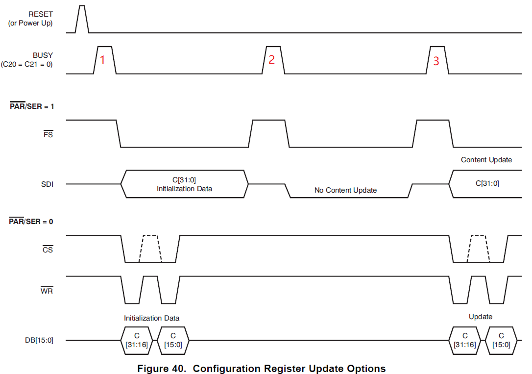
    After you send correct command to ADS8528, send two CONVST_x pulses to ADC which is required to update the register, please refer Figure 40 (busy signals) and the description about bit 30 of CR register(two accesses for reading).

    Regards

    Dale

  • Hi Dale,

    many thanks for your help.

    I am not sure, but can you please check, if it is really two CONVST_x pulses - I think you mean that we have to send 2 times all 32 Bits of the configuration register - and this is done by two pulses of CS.

    My secound question is:

    We conneted all CONVST_x signals together with the CS signal. This means after I read the results, I will set the CS high and this will trigger the next ADC-conversion. If we write the config register, I have to write the first time (2x 16 Bits) - after that I will bring CS high. This means I set CONVST_x signals to high, which means ADC-Conversion will be done - after that I will write the 2x16Bits of configuration register the second time.

    We will not use the next ADC-results - but can you tell me if you see here a problem, that we have a conversion between the writes to config register.

    regards

    Juergen

  • Hello Juergen,


    I will check the detail and get back to you soon. Thanks.


    Regards


    Dale
  • Hello Juergen,

    I apologized for late response.

    It needs two CONVST_x, please check the timing as below, there are two BUSY signals after writing the command, which means two CONVST_x signals.

    Independent /CS signal will make the timing simple. Based on your description, you missed one CONVST_x(BUSY 3) signal between your two 2x16bits register writings. Please check the timing as below.

    Also, the command you wrote to ADC is not the command what you want, please see my previous response.

    Thanks.

    Best ragrds

    Dale

  • Dear Dale,

    in the meantime we were able to solve our Problems. One of the causes was that we had connected all CONVST_x signals together with the CS Signal as one Signal. Now we create all of these signals separately.

    Many thanks for your assistance.

    Best regards 

    Christian Zellner