This thread has been locked.

If you have a related question, please click the "Ask a related question" button in the top right corner. The newly created question will be automatically linked to this question.

ADC12D1600: Data from the ADC is not correct.

Part Number: ADC12D1600
Other Parts Discussed in Thread: , ADC08D1500

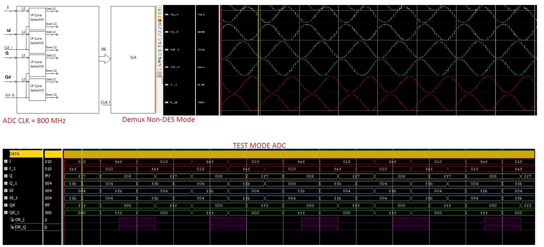
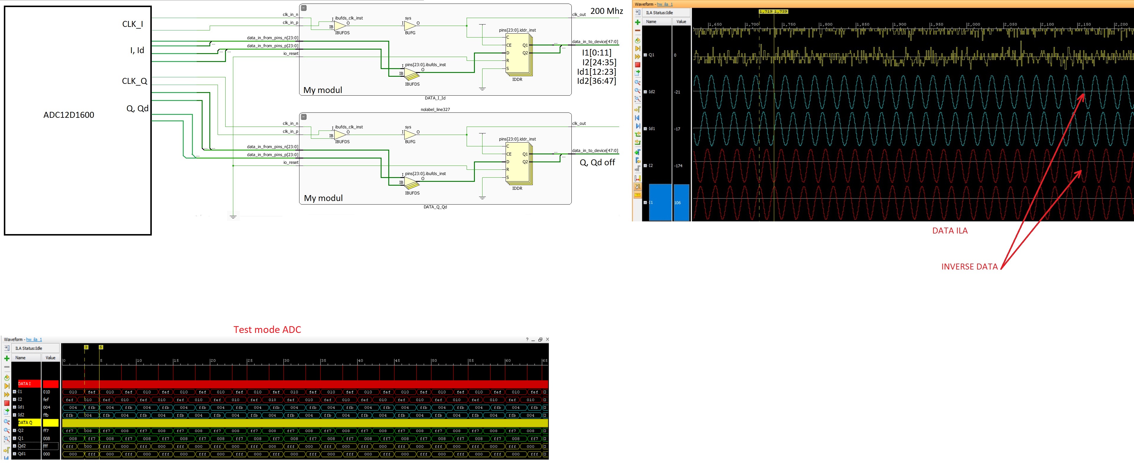
The ADC receives a clock frequency of 800 MHz. ADC Demux Non-DES Mode.
CAL_ADC = 0
DDRPH_ADC = 0
ECE_ADC = 0
CALDLY_ADC = 0
FSR_ADC = 0
NDM_ADC = 0
TPM_ADC = 0
PDI_ADC = 0
PDQ_ADC = 0
DES_ADC = 0
Configuration register 0x2010. CLK_I and CLK_Q 200 MHz. Data is sent to SelectIO. I connected to the output of SelectIO ILA. I get odd data inverted. ADC test mode data is correct.

  • Hi Nikola,

    One of our experts is taking a look into your issue, and will be back with you shortly.

    Best Regards,

    Dan
  • Hi Nikola
    That ADC has four output data ports. Each data port has 12 LVDS differential pair outputs. It sounds like you are processing the positive and negative signals from each differential pair separately. The negative signal from each differential pair will be inverted with respect to the positive signal. I presume you have all of the negative signals connected to the odd channels of your SelectIO inputs.
    Can you change the SelectIO configuration so the inputs are configured as LVDS pairs? That way you will get one logical input for each pair of SelectIO inputs, corresponding to each ADC LVDS output pair?
    Best regards,
    Jim B
  • Hello Jim! Jim, thanks! You helped me well. I understood what was going on. The input SelectIO data bus is limited. The bus can not be more than 16 bits. It is necessary to use 4 SelectIO components in channels I, Id, Q, Qd. I wanted to use the differential frequency CLK _I and CLK _Q. Vivado does not allow to connect differential conductors to several components. I connected the differential wire CLK _I_diff and CLK_Q_diff using BUFDS. I received a non-differential CLK_I and CLK_Q. CLK_I is connected to SelectIO_I and SelectIO_Id. CLK_Q is connected to SelectIO_Q and SelectIO_Qd. I do not need to use SelectIO? I need your help on how to properly process data from the ADC. Do you have sample code?

  • Hi Nikola

    Please see the FPGA firmware source contained in the ADC12D1600RB/ADC12D1800RB Design Package which is available in the software section of this web page:

    http://www.ti.com/tool/adc12d1600rb

    I believe in this firmware only one of the DCLK inputs is used to clock all 4 banks of data into the FPGA.

    I hope this is helpful.

    Best regards,

    Jim B

  • Hello Friend! I changed my project. I created a component with 24 differential inputs and 48 output data buses. Data from channels I and Id are fed to the input. Differential clock CLK_I is connected to the input for data I and Id. Differential clock CLK_Q is connected to the input for data Q and Qd. I turned off the channel Q. Data is transmitted only on the I and I channel. Replacing the IP core of the SelectIO did not change the result. The data channel is inverse between measurements. I turned on the ADC test mode to check the channels. The test is normal. What is the problem? If the FPGA does not work correctly, why does the test pass normally?

    I looked at the data from the ADC. I sent the channel I data to ILA. To view the data that is negedge clk_I, I recorded the data in a 12-bit register clocked negedge clk_I. I sent the recorded data to ILA. The result is the same. Even and odd data are inverse.

  • Hi Nikola
    Each LVDS pair that is input to the FPGA should be captured in a latch. The output of the latch will be a single bit, not 2 bits. You should end up with I[0:11], Id[0:11], Q[0:11], Qd[0:11]. I think that initial differential to single bit logic is handled in the adc1k_if.v source code in the design package information I referred to earlier.
    If you are handling the negative signal of each LVDS pair as a separate logical signal it will appear inverted with respect to the corresponding positive signal from the same LVDS pair.
    Best regards,
    Jim B
  • Hi Jim! I studied your examples. I accept the data from the ADC as in your example. Your example uses BUFDS and IDDR. I do that too. I in the message above loaded the scheme of the project. I tried a different design. I tried IP core XILINX. I tried my modules. I tried to look at the data from BUFDS. I always got the same result. The problem is not in FPGA. How do I check the ADC? Mode other than TEST MODE? This mode will not show fully the operation of the ADC. In this mode, the ADC sends a number and an investment number.

  • Hi Nikola
    What is the frequency of the applied analog input signal?
    I recommend using a frequency that is fairly low for initial testing, perhaps 50 MHz or so. A low frequency tone usually makes it easier to sort out any data ordering or mapping issues in the capture logic.
    Once I know the frequency you are inputting I will use an ADC12D1600 board connected to a logic analyzer to capture representative data to compare with your setup.
    Best regards,
    Jim B
  • Hi Nikola
    Have you made any progress on this issue?
    Can you provide the information I requested in my previous post, so I can replicate your setup and provide data captured from the ADC outputs using a logic analyzer?
    Thanks!
    Best regards,
    Jim B
  • Hi Jim! Sorry for not immediately answering, I was busy. I put aside this board with ADC12D1600 ADC. I have a board with ADC ADC08D1500 and FPGA. I decided to check correctly I accept the data from the ADC. This ADC is similar to the ADC12D1600, it is only 8 bit, the speed is lower and the control is slightly different. I checked my design. I received the correct data in DDR mode. Now I’m sure that I’m doing everything right. I checked the connection of the ADC and PCB.
    My ADC12D1600 Sampling Clock CLK = 800MHz data clk DCLK = 200 MHz. I connected DCLK to the pin FPGA DCLK = 200MHz and measured the frequency on the pin. I will try to lower the Sampling Clock. At 50 Mhz, should I set bit 8 in the Configuration Register?

  • Hi Nikola
    Please let me know how things work with a reduced ADC clock frequency.
    For best ADC performance change LFS to 1 for ADC clock frequencies below 300 MHz. This won't affect the output test pattern, but will improve ADC performance with real input signals.
    Best regards,
    Jim B
  • Hi Nikola
    I'm going to mark this as resolved for now.
    If you are still having issues with data capture please let me know.
    Best regards,
    Jim B
  • Hi Jim! I solved the problem. The synthesizer did not set the necessary frequency. Incorrect frequency posumala on demodulator. Since the demodulator is not the correct data received on the ADC. Thanks for the help. Now everything is working fine.