This thread has been locked.

If you have a related question, please click the "Ask a related question" button in the top right corner. The newly created question will be automatically linked to this question.

ADS1256: ADS1256 Register Read Write Issue.

Part Number: ADS1256

  Hi,

I have ADS1256 ADC module, which is interfaced with a STM32F746,

I stared with a Read Registers default values are ok as per data Sheet but when i write any value to any register MSB i.e bit7 is always '1' while reading,

for eg.

DRATE: A/D Data Rate (Address 03h)

if i write a 0x33 that is 00110011---15SPS

while reading i always get a 0xb3 that is 10110011,

similarly for all register read bit 7 is always '1' 

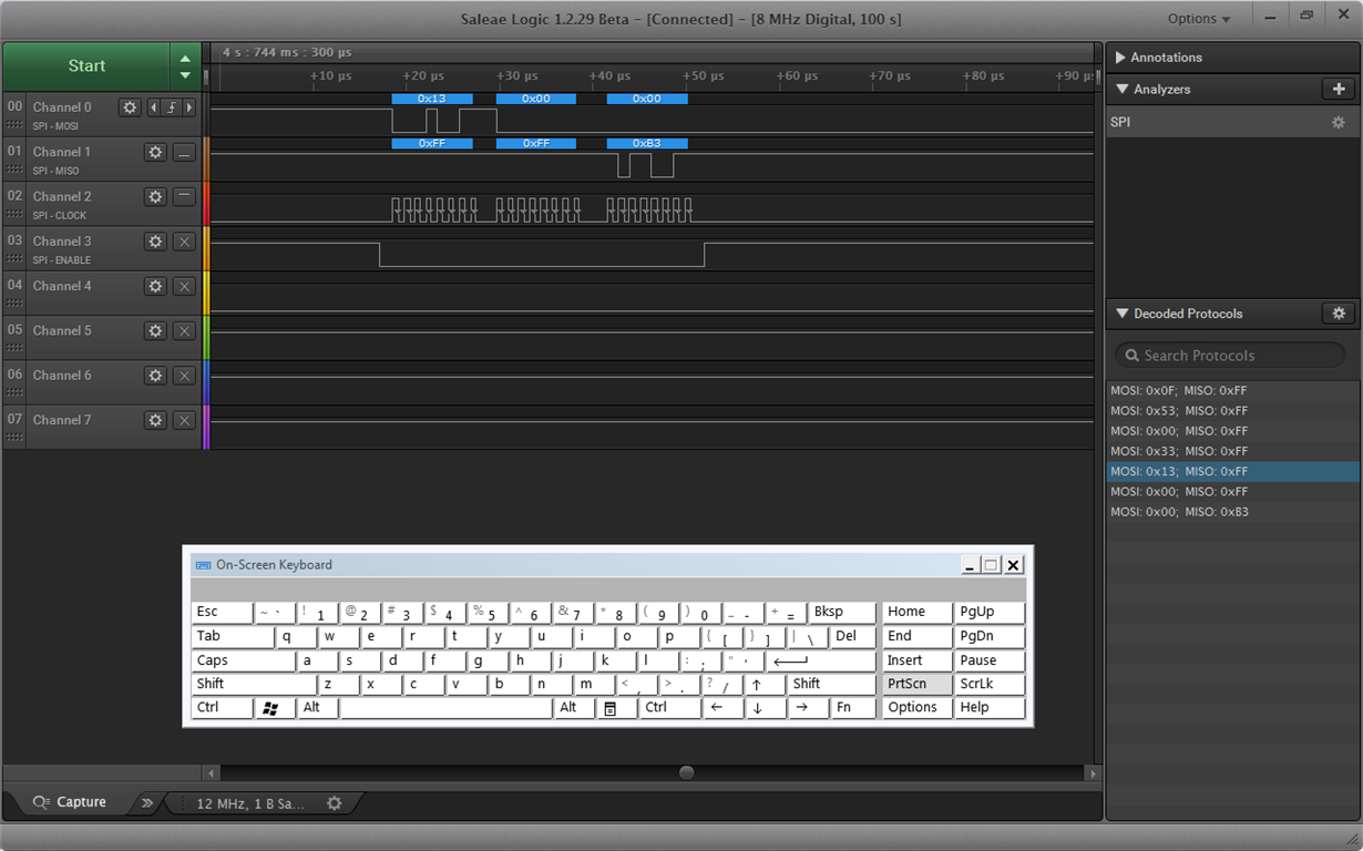
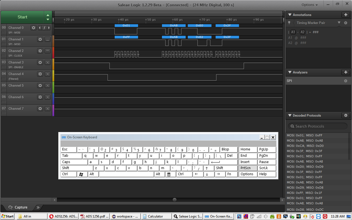
please find the attached logic analyzer Screen shots

Thank you.


  • Hi Vikas,

    With the ADS1256, some commands have to insert delays between the command input and data retrieval. The RREG command is one of them - please refer to the RREG description on page 36 and figure 34. From your screen capture above (thank you for that by the way!) I can't tell if you are meeting the t6 delay before sending the second 0x00. The t6 delay is defined in the Timing Characteristics table on page 6 of the datasheet.
  • Hi Tom,

    it Seems t6 delay was not correct 

    from data sheet,

    t6
    Delay from last SCLK edge for DIN to first SCLK rising edge for DOUT: RDATA, RDATAC,
    RREG Commands


    50 τCLKIN

    the master clock period is 0.625us * 50 = 31.25us -- t6 delay

    after 0x00 second command to read register i apply delay of 32us, now read register seems OK, i checked repeatability, seems OK,

    Is that correct t6 delay, i am not getting correct data with t6, please correct.

    thank you,

    vikas.

  • Hi Vikas,

    Let me see if I understand, when you add the delay after the RREG command you are getting proper data for the register detail, is that right? But with that delay, you are not getting proper conversion data? Is that the case?
  • Hi Vikas,

    When you say the master clock period is "0.625 us", does this mean you are applying a 1.6 MHz external clock source to the CLKIN pin? What is your master clock frequency?

    7.68 MHz is the nominal master clock frequency for this device. Also, the SCLK frequency must not exceed 4*τCLKIN.

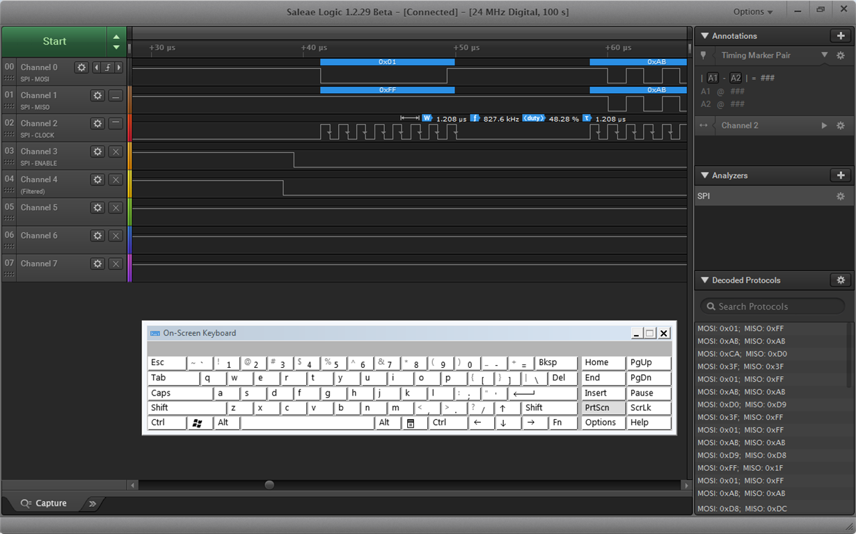
    Therefore, if fCLKIN is 7.86 MHz, then SCLK should not exceed 1.92 MHz. In case of a 1.6 MHz master clock, then SCLK should not exceed 400 kHz, which would seem to be in violation of the ~800kHz SCLK frequency that I estimated from the logic analyzer screenshot. Let me know if got your clock frequencies correct or not...

    If you could share another screenshot with the read data (RDATA) SPI command, it would be helpful. Also, let us know what your input and reference voltages are. Thanks!
  • Hi chris,

    Reading and writing registers are Ok

    having trouble with read correct data continuous 0x03 and in single shot mode 0x01. 

    Clock is at 830 kHz

    while reading data, i getting a random values every time and after some time say after 30-50 sec continuous read get stopped and output is always a 16777215 -0xffffff

    i am planning to read single ended ch1-ain0 

    adc config are - status is at 0xf0 where upper nibbles xxxx

    reg mux is at 0x0f

    reg adcon is at 0x20

    reg drate is at 0x03 -- lowest data rate for now

    Program SPI Config 
    
    hspi2.Instance = SPI2;
    hspi2.Init.Mode = SPI_MODE_MASTER;
    hspi2.Init.Direction = SPI_DIRECTION_2LINES;
    hspi2.Init.DataSize = SPI_DATASIZE_8BIT;
    hspi2.Init.CLKPolarity = SPI_POLARITY_LOW;
    hspi2.Init.CLKPhase = SPI_PHASE_2EDGE;
    hspi2.Init.NSS = SPI_NSS_SOFT;
    hspi2.Init.BaudRatePrescaler = SPI_BAUDRATEPRESCALER_64; //-----------------------------844kbits/sec
    hspi2.Init.FirstBit = SPI_FIRSTBIT_MSB;
    hspi2.Init.TIMode = SPI_TIMODE_DISABLE;
    hspi2.Init.CRCCalculation = SPI_CRCCALCULATION_DISABLE;
    hspi2.Init.CRCPolynomial = 7;
    hspi2.Init.CRCLength = SPI_CRC_LENGTH_DATASIZE;
    hspi2.Init.NSSPMode = SPI_NSS_PULSE_DISABLE;


    i am not understanding "1.6 MHz master clock, then SCLK should not exceed 400 kHz

    should i lower the clock frequency since as in screen shot while read and write clock seems at 830 kHz

    Please Correct.

    Thank you. 


  • Hi Vikas,

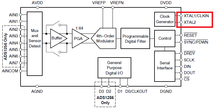
    When asking about the master clock frequency (fCLKIN), I am wondering what you have connected to the XTAL1/CLKIN and XTAL2 pins. Are you clocking the ADS1256 from a crystal, or are you using an external clock source connected to the XTAL1/CLKIN pin? What frequency is this clock?

    The SCLK signal is a separate signal used for serial communication; however, the maximum SCLK frequency is limited to 1/4th the clock frequency of the ADC's master clock frequency.

    Thank you for the additional screenshots. One thing I noticed is that while clocking out hte data, you appear to be sending random commands to the ADC. I would recommend that after the RDATA command (0x03) you only send WAKEUP (0x00) commands (these are equivalent to NOP) while clocking out the data: