Other Parts Discussed in Thread: LMX2592
hello,Jim
we are testing DAC38RF82 now, we face some problems and need your help;
Firstly,Project Requirements:
1.FDac(DACCLK)=7200M,External Diff Clk;
2.Single DAC(DAC A)
3. 1 IQ pairs
4. 8 serdes lanes
5.Interprolation=6
6.output IF analog signal=1.7GHz
7.LMFSHD=82121
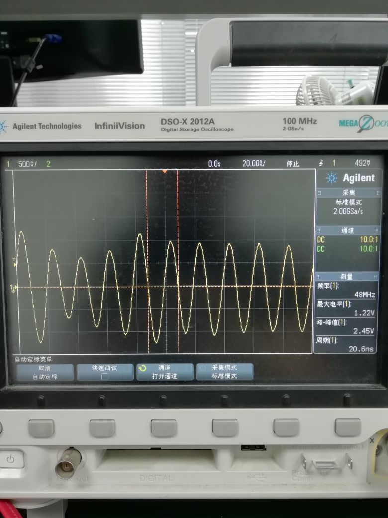
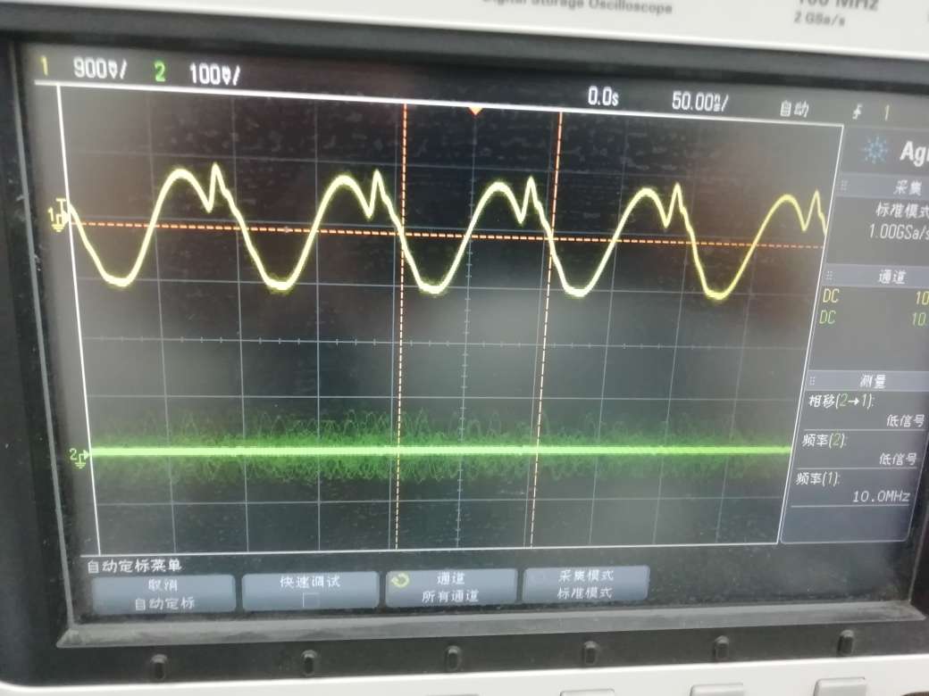
8.sysref=10MHz
9.FPGA GTH refclk=150MHz
Secondly,Our DAC38RF82 register configuration :
address data
0x00 0x7860
0x01 0x1880
0x40A 0x7003
0x40B
0x40C
0x423 0x03F3
0x424 0x1000
0x431 0x0200
0x43B 0x1002
0x43C 0x0029
0x43E 0x0929
0x10A 0x83B0
0x10C 0x2422
0x10D 0x8300
0x10F 0x1F83
0x11C 0x0000
0x11E 0x71C7
0x11F 0xC71C
0x120 0x3C71
0x124 0x0020
0x125 0x6300
0x127 0x2124
0x128 0x0100
0x130 0x0000
0x132 0x0800
0x146 0x0044
0x147 0x190A
0x148 0x31C3
0x14A 0xFF03
0x14B 0x1300
0x14C 0x1307
0x14D 0x0101
0x14E 0x0F4F
0x14F 0x1CC1
0x150 0x0000
0x151 0x00FF
0x152 0x00FF
0x15C 0x0003
0x15F 0x3210
0x160 0x5764
The Problems:
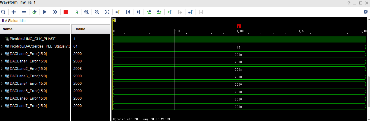
1. We read register 0x64 to 0x6D ,the result as below(DACLANE0_Error ~ DACLANE7_Error)
DACLANE0_Error ~ DACLANE7_Error=0x2000
DACLANE2_Error =0x2008
2.The JESD204B Link chain between DAC and FPGA is always attemping to establish