This thread has been locked.

If you have a related question, please click the "Ask a related question" button in the top right corner. The newly created question will be automatically linked to this question.

ADS8168: Problems with Custom Channel Sequencing mode

Part Number: ADS8168

Hello,

I'm trying to test the ADS8168 with Custom Channel Sequencing mode, which for some reason doesn't work.

I'm using a custom board with an ADS8168 on it and another custom board with an ARM processor on it, controlling the ADS8168 via SPI.

Manual mode and auto sequence mode works already very fine, so I think it's not a problem with the timings nor with the SPI mode (we're using SPI-01, by the way).

I'm trying the following configuration:

- Set ADS8168 to custom channel sequence mode

- Define channels 0 and 1

- Set sequence start to index 0 and end to index 1

- Start the sequence

- Discard first answer

- Read two answers

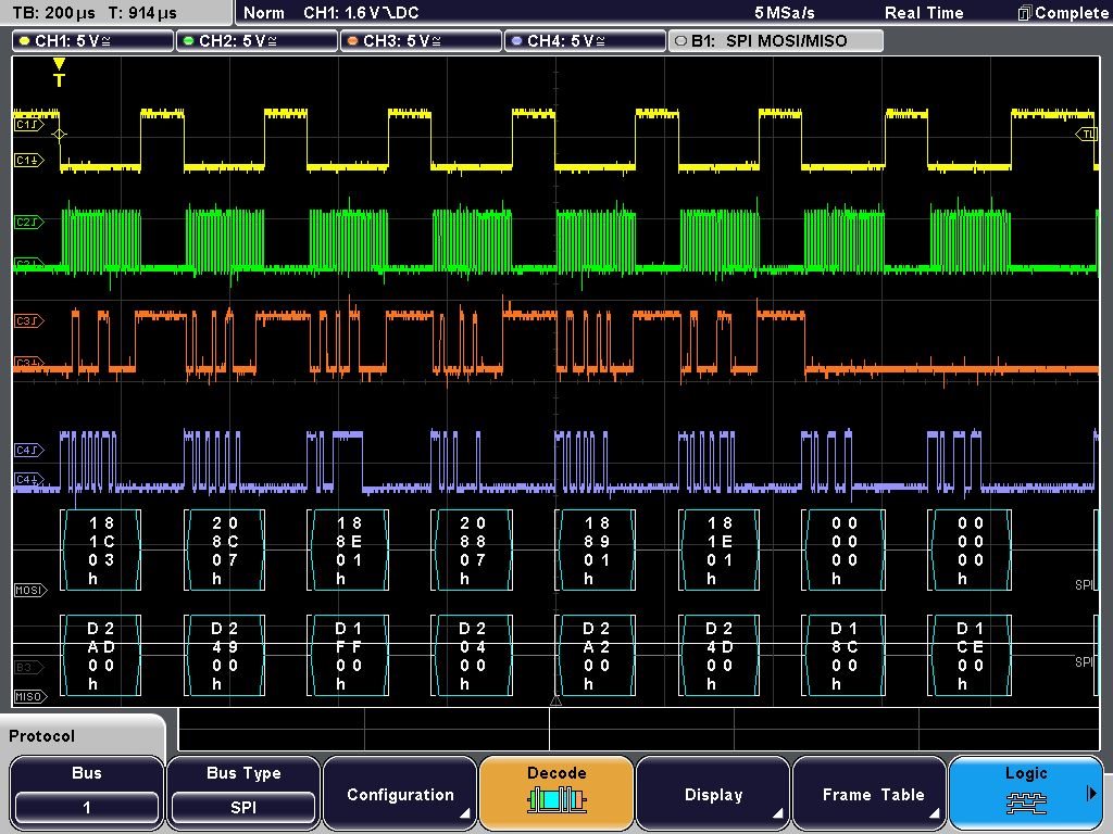
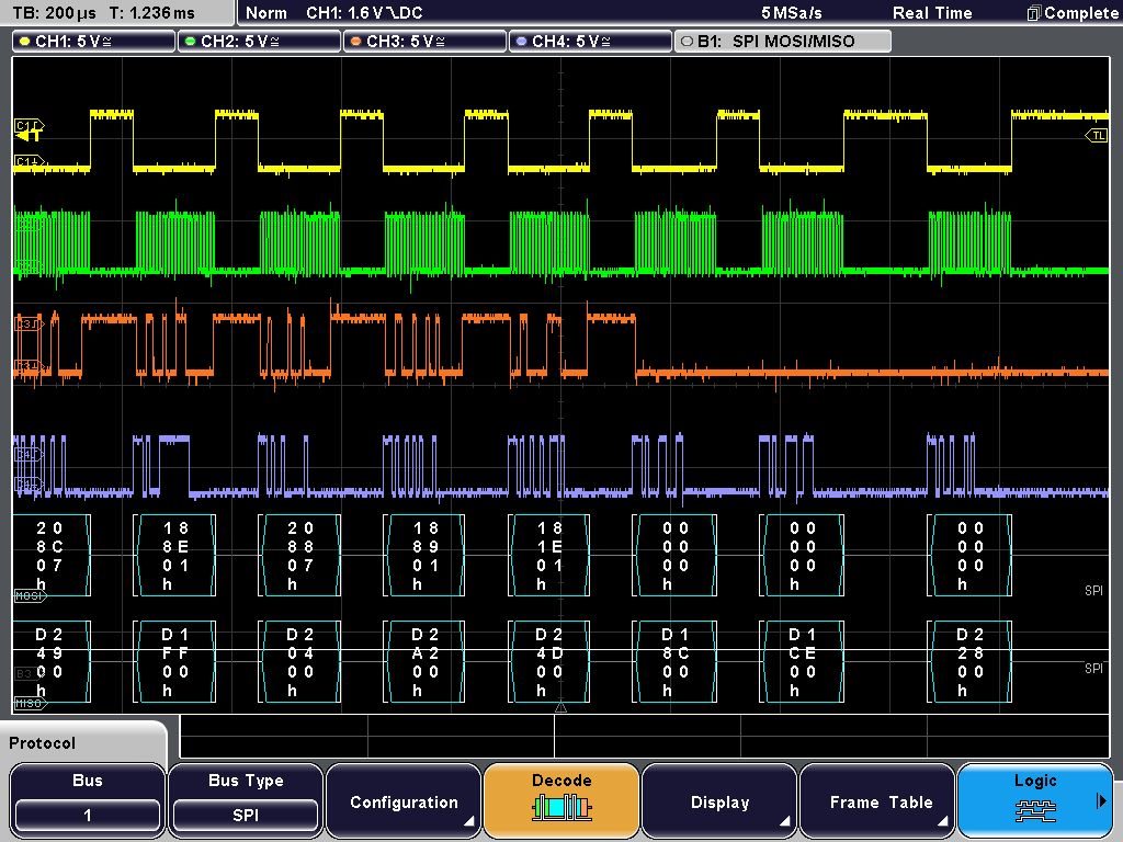
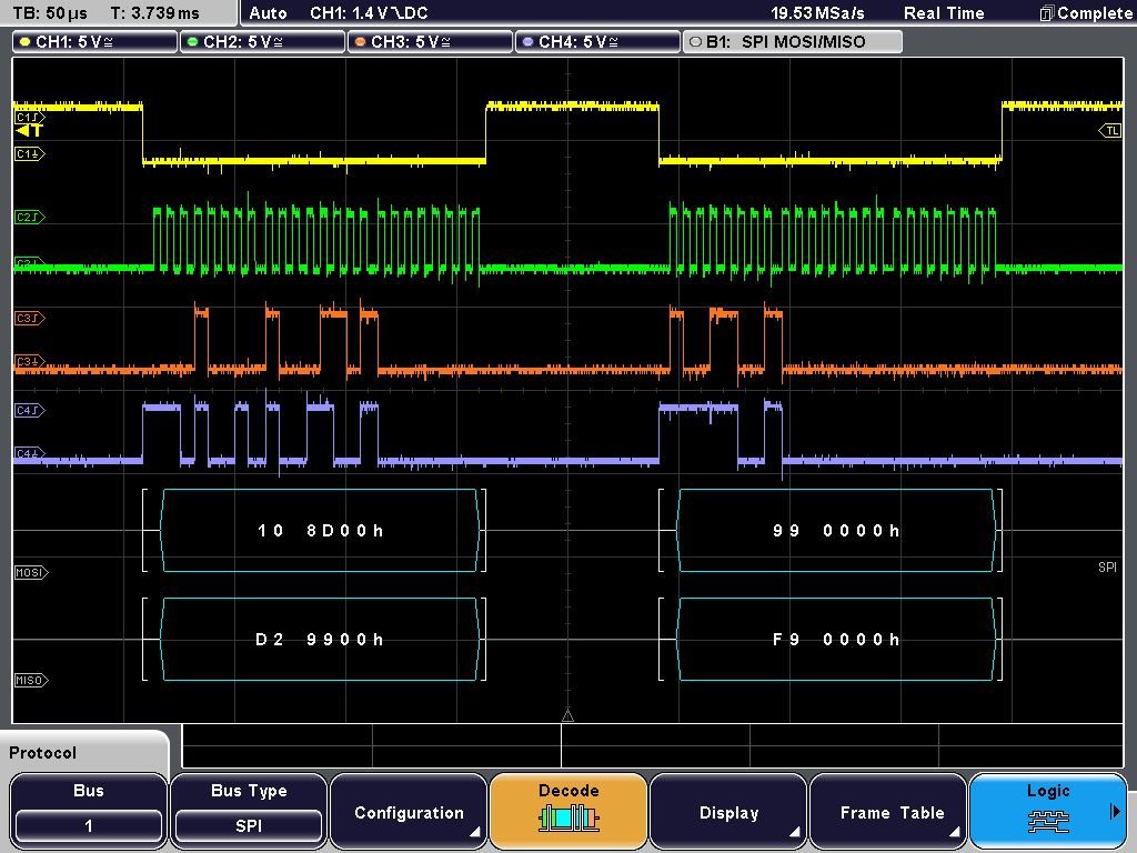
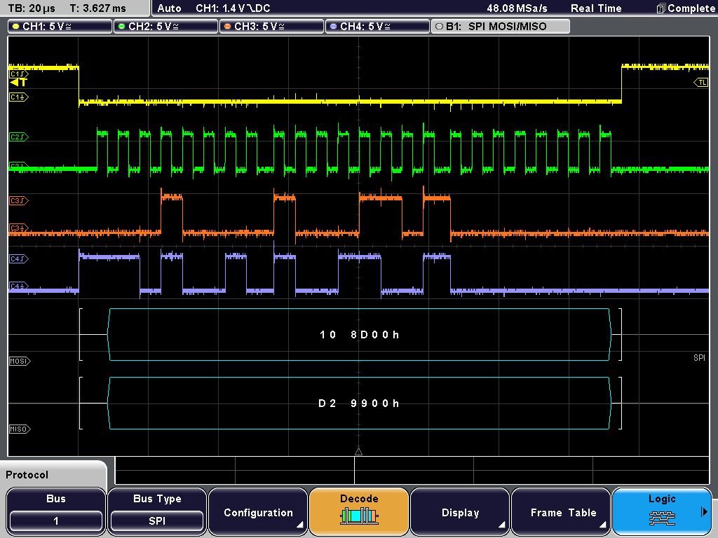
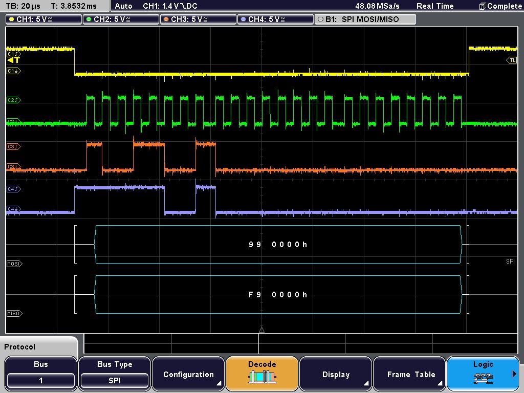
The second scope screenshot is only to see the second answer.

See the decoded SPI messages on the bottom of the scope screens.

Analog input values:

AIN0: 3.359V

AIN1: 0.343V

So, the first answer seems ok - the ADC value is 0xD1CE. However, the second answer is about the the same value, which is not ok. It seems the multiplexer doesn't switch the channels (checked with scope on ADC-INP), everything else seems to be fine.

Any ideas what could be the problem here?

Kind regards,

Markus

  • For some reason, the images (using only copy & paste) made it only into the board editor, but not into the actual post...

    So, I'm gonna try it with the "insert function"...

  • Hi Markus,

    Thank you for including the timing wave forms.  

    I think you may be off by 1 bit.  In the first frame, where you write to the Device_CFG register, you are writing 0x181C03.

    If I read the data sheet correctly, in order to write to a register, the correct sequence would be 0x081C03.  In Table 8, the 5 bit WR_REG command is 00001b followed by the 11 bit address and the 8 bit data.

    Regards,
    Keith Nicholas
    Precision ADC Applications

  • Hello Keith,

    thanks for your answer.

    Since for the most registers that I want to write to, writing to other bits is prohibited according to the datasheet (e.g. bits 7-4 in the DEVICE_CFG register - according to table 31), I mostly use the "SET_BITS" command, which is coded as "0x00011" and the "CLR_BITS" command ("0x00100"). So, as I see it, 0x181C03 should be correct.

    Or did I get something wrong here?

    Also, is it safe (against my understanding of the data sheet) to use the "WR_REG" command for writing registers which contain "don't write to these bits" bits?

    Kind regards,

    Markus

  • Reading out the used registers, I get the following:

    ----------

    ADS8168_REG_DEVICE_CFG (0x1C) = 0x03

    Register 0x8C = 0x00

    Register 0x8E = 0x01

    ADS8168_REG_CCS_START_INDEX (0x88) = 0x00

    ADS8168_REG_CCS_END_INDEX (0x89) = 0x01

    ADS8168_REG_SEQ_START (0x1E) = 0x00

    ----------

    The values seem to be correct in my eyes.

    This is before starting the sequence, so the value for the ADS8168_REG_SEQ_START seems to be correct, too.

    Any ideas what could be missing?

    Kind regards,

    Markus

  • Reading out also other (not-written-to) register:

    ----------

    ADS8168_REG_DEVICE_CFG (0x1C) = 0x03

    Register 0x8C = 0x00

    Register 0x8D = 0xFF

    Register 0x8E = 0x01

    Register 0x8F = 0xFF

    ADS8168_REG_CCS_START_INDEX (0x88) = 0x00

    ADS8168_REG_CCS_END_INDEX (0x89) = 0x09

    ADS8168_REG_CCS_SEQ_LOOP (0x8B) = 0x00

    ADS8168_REG_SEQ_START (0x1E) = 0x00

    Channel 0: 53804 => 3.362801V

    Channel 1: 53682 => 3.355176V

    ----------

    Setting now also 0x8D and 0x8F explicitly

    => strange result:

    ----------

    ADS8168_REG_DEVICE_CFG (0x1C) = 0x03

    Register 0x8C = 0x00

    Register 0x8D = 0xF9

    Register 0x8E = 0x01

    Register 0x8F = 0xF9

    ADS8168_REG_CCS_START_INDEX (0x88) = 0x00

    ADS8168_REG_CCS_END_INDEX (0x89) = 0x09

    ADS8168_REG_CCS_SEQ_LOOP (0x8B) = 0x00

    ADS8168_REG_SEQ_START (0x1E) = 0x00

    Channel 0: 53813 => 3.363364V

    Channel 1: 53789 => 3.361864V

    ----------


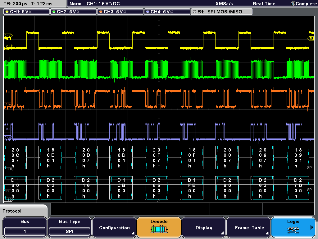
    However, checking setting the registers it should be correct:

    0x208F07 => Clear bits 0b111 of register 0x8F

    0x188F01 => Set bit 0x001 of register 0x8F

    0x208907 => Clear bits 0b111 of register 0x89

    0x188901 => Set bit 0x001 of register 0x89


    Also, the readouts are correctly read:

    Quite strange...

    Kind regards,

    Markus

  • Hi Markus,

    You did not misunderstand; I was too quick with my previous answer and overlooked the do-not-write bits.  Use the SET bits and CLR bits commands when writing to registers with read-only (do-not-write) bits.

    Based on what you have provided, I do not think you are missing anything. Registers = 8D, 8F, 91, 93, 95, 97, 99, 9B, 9D, 9F, A1, A3, A5, A7, A9, and ABh should read default value of 01h, not FFh.

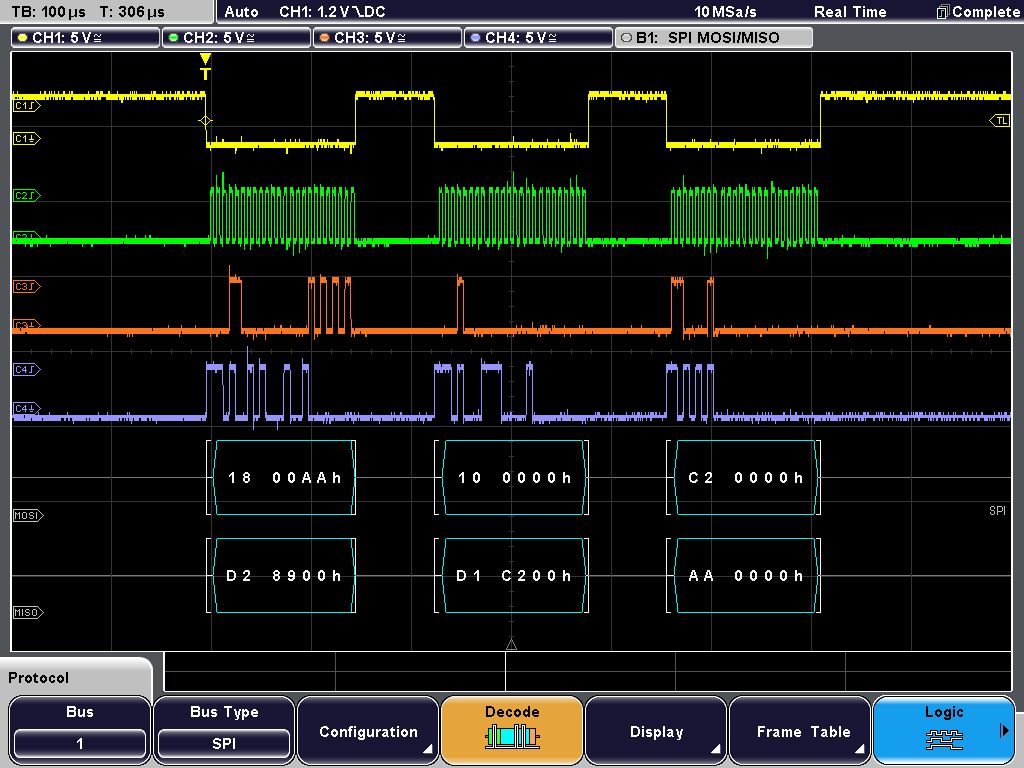
    I think your timing and commands are correct, but to make sure on the timing, can you send a zoomed version of the read frame for register 8Dh?  I want to check all of the setup and hold times.

    Assuming you are meeting all timing requirements (I do think you are since you can get the other channel sequence modes to work) , please give me a few days to follow-up with the design team.  

    Regards,
    Keith

  • Hello Keith,

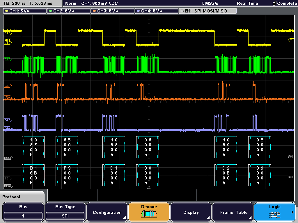
    here are the "zoomed-in" scope images for the access to the 0x8D register:

    Great if you can have a look at it with the design team!

    Kind regards,

    Markus

  • Hi Markus,

    I am not sure if this is needed, but to test the interface, please try the following (if you are not already doing this).

    1) write 0xAA to address 0x00 to enable register write access.

    2) Write to address 0x00 - using both SET_BITs and REG_WR opcodes, and then read back register to verify.

    Thanks,

    Keith

  • Hello Keith,

    Writing 0xAA to 0x00 register (using REG_WR)


    Writing 0xAA to 0x00 register (using SET_BITS)

    Seems ok to me.

    Maybe you have also an ADS8168 eval board around and can check the outcome when using the same commands I use (for setting up custom channel mode)?

    Kind regards,

    Markus

  • Hi Markus,

    I will look at this on one of our EVM's, but I will not be able to until early next week.

    Regards,
    Keith

  • Hi Markus,

    I spent some time today looking at the EVM and it does appear that the REPEAT_INDEX_m registers default to 0xFF, not 0x01.  These are full 8 bit registers, so you need to write to all 8 bits and update from 1111 1111b to 0000 0001b.  You can do this using the WR_REG command, or first clearing all bits using the CLR_BITS command and then setting the desired bits.

    For example, to update register 0x8D to 1:

    08 8D 01h  (WR_REG)

    OR

    20 8D FFh  (CLR_BITS)

    18 8D 01h  (SET_BITS)

    Also, you are already doing this correctly, but do not set the SEQ_START bit until all of the other registers have been properly configured for Custom Channel Sequence mode.  I inadvertently did this using the EVM, and then could not get the channel sequencing to work correctly.

    Regards,
    Keith

  • Hi Keith,

    thanks - this solved my problem! Custom sequence is running now!

    So, maybe you want to put/correct this information in the data sheet (and eventually also provide a working example) in order to help other developers get it up and running more quickly.

    Kind regards and again many thanks,

    Markus