This thread has been locked.

If you have a related question, please click the "Ask a related question" button in the top right corner. The newly created question will be automatically linked to this question.

ADS1299: DC Lead Off Detection Questions

Part Number: ADS1299

Dear TI Experts:

We have configured a 64 channel system with 8 TI chips in a referential montage.  We are using 64 P inputs, single reference electrode using SRB1 connected to all chips, bias electrode with PD_BIAS enabled only on one chip and BIAS_SENSP/BIAS_SENSN enabled on all channels.

We have configured DC lead off detection at 24 nA, set the comparator thresholds to 70%/30%, and have enabled LOFF_SENSP for all channels.  We're logging the status bits from each channel for lead off status.

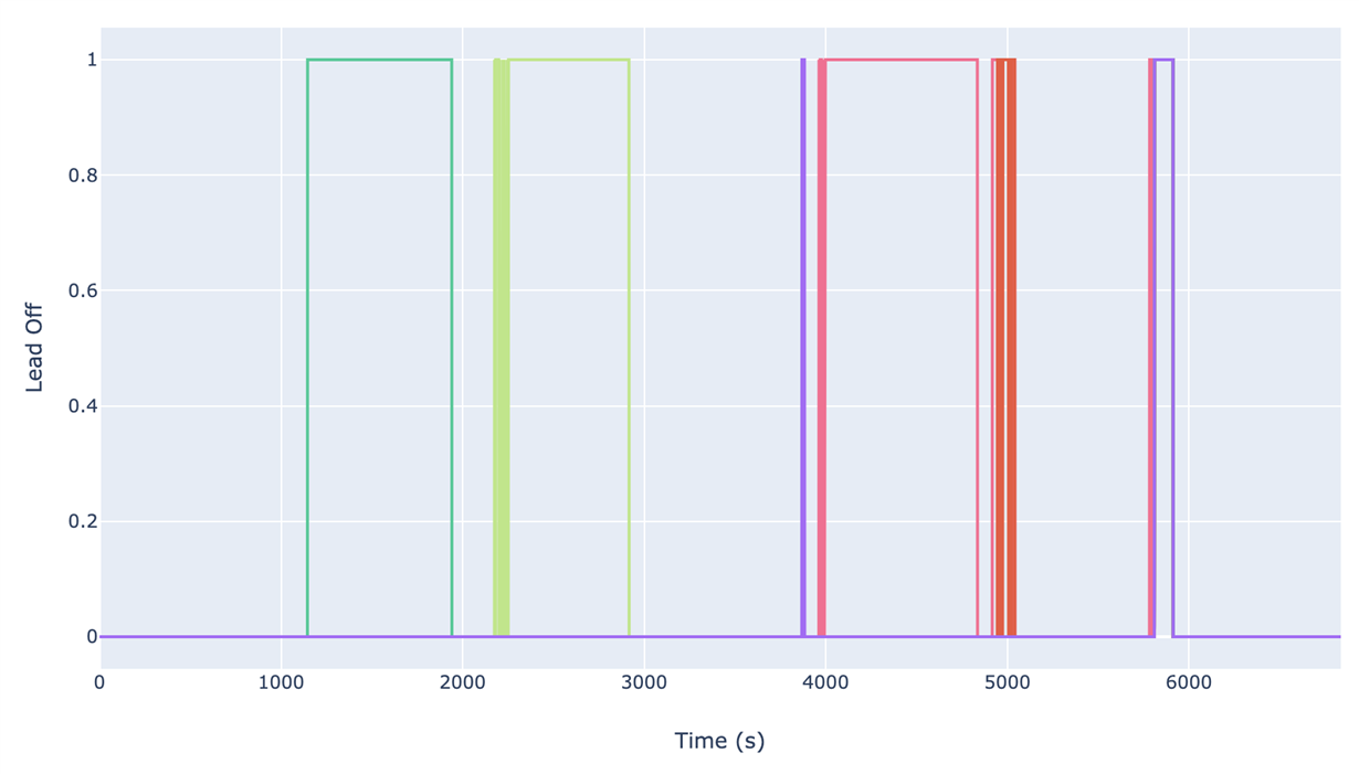
1) Even though we're seeing the expected behavior when an electrode is removed, the comparators do not consistently indicate lead off events (see figures below).  Is this expected?

2) Since the mux disconnects the SRB1 from the lead-off current source, can we physically connect the SRB1 to one of the N inputs to access the current sink from that channel and use the comparators on that channel for lead-off status of the reference electrode simultaneously with all other electrodes?

3) Shouldn't the bias be trying to correct and DC offset introduced by the lead off current sources?  Would there be any difference if we disable BIAS_SENSP/BIAS_SENSN?

  • Hi Alex,

    Thank you for your post and welcome to our forum!

    There might be a couple things going on which may affect the BIAS amplifier and lead-off detection:

    1. The BIAS amplifier output may be saturating. Each BIAS_SENSx bit connects another 220k resistor in parallel at the BIASINV summing junction. This effectively reduces the Rg resistance of the amplifier feedback network, which increases the amplifier closed-loop gain. Having all BIAS_SENSP pins enabled may be saturating the BIAS amplifier. I would suggest starting with only a few electrodes strategically placed to cover the entire measurement area. This should be all that's needed to derive the common-mode signal on the body.
    2. While establishing the common-mode on the body, the BIAS amplifier is also responsible for sinking/sourcing any imbalanced current from the lead-off current sources. If all LOFF_SENSP bits are enabled and none of the LOFF_SENSN bits are enabled (rightfully so, as you are using SRB1 instead), then all the current (16x i_LOFF) must return through the BIAS amplifier. This could saturate the amplifier as well, depending on the current magnitude and any impedance in the path. If the DC common-mode fluctuates, it may produce unreliable LOFF comparator results. I don't believe I see an issue with connecting the SRB1 input with the INxN pins to access the negative LOFF current sources and comparators.

    Keep in mind that the BIAS amplifier does not correct for DC offset. Instead, it establishes a DC common-mode voltage for all electrode inputs. It also senses and cancels some of the AC common-mode noise. DC offset can still be caused by differences in input impedance and current on each input.

    Best regards,

  • Thanks for the quick reply Ryan!  Makes sense.

    Do you know what frequencies of AC common-mode noise the bias sense and tries to cancel?  Will it try to cancel out low frequency noise or just higher frequency 50/60 Hz?

  • Hi Alex,

    The RLD loop will attempt to correct for any frequencies within the closed-loop bandwidth of the system. How effective this approach is depends on the gain, which varies across frequency. At DC, the gain is set purely by Rf and the summing junction of 220k resistors inside the device. The gain will continue to roll off as frequency increases.

    Check out an FAQ post on this topic as well as other helpful topics on our ADS129x BIOFAQ page.

    https://e2e.ti.com/support/data-converters/f/73/t/772010

    Best regards,