This thread has been locked.

If you have a related question, please click the "Ask a related question" button in the top right corner. The newly created question will be automatically linked to this question.

ADS131A04EVM: Configuration Commands Accepted For Async Interrupt Mode. However, the device responds back with all zeroes on first data cycle. Then DRDY doesn't go low again

Part Number: ADS131A04EVM

Hi there, I am using the eval kit with an FPGA wired in as the master and am experiencing some trouble with the ADC not giving me data on the first DRDY falling edge. Then I don't see DRDY come back down low so I am wondering if I have a setting incorrect somewhere:


I have the following settings for asynchronous interrupt mode with +/-2.5V input voltage:

JP1: Installed to allow FPGA to be the master

I am using the USB power so left the JP2 and JP3 jumpers as is

JP5: 1-2:  (M0: IOVDD Asynchronous interrupt mode)

JP6: 2-3  (M1 : GND 24 bit)

JP7: I tried both 2-3 and float and received same results. (M2 hamming code disable)

JP8: Uninstalled (Charge pump of)

JP9: Tried both installed and uninstalled. (use onboard reference)

JP10: Uninstalled (Use on board IOVDD)

JP11: 2-3 (Use +/-2.5V supplies)

I am using the following config process to enable the ADC for 4096 Oversampling to give me a 4KHZ sampling rate in asynchronous interrupt mode. Let me know if there is an incorrect setting in the CFG:

Send Null Command: 0x000000

Send Unlock Command: 0x065500

Send SYS_CFG_REG Write: 0x4B6800

Send CLK1_REG Write: 0x4D0000

Send CLK2_REG Write: 0x4D0000

Send ADC_EN Register Write: 0x4F0F00

Send Wakeup Command: 0x003300

Send Lock Register Command: 0x055500

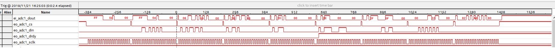
Send Null Command: 0x000000    (I get every response up to here correct and you can see that in the logic analyzer shot)

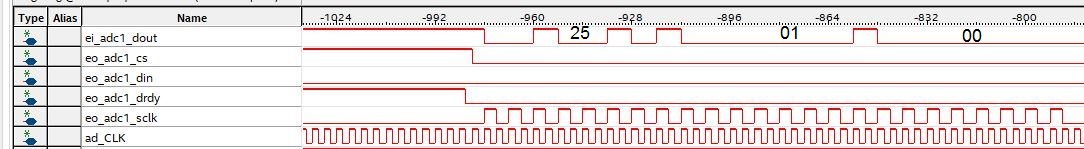
Wait until the ADC pulls DRDY low and then go and read all the channel data. When I read the data, I get the Lock register command back as the status but flatlined DIN for the 4 channels of data. When I keep the ADC as is and reset the FPGA to restart the initialization routine, I and only then see the correct data from the ADC after DRDY goes low. Then after this read, I don't see DRDY come back low again.

This is the initialization:

This is the first data read:

  • Tony,


    It's not very clearly spelled out in the datasheet, but when a conversion completes, the /DRDY is indicated. However, the conversion is put into a data buffer and that /DRDY period afterwards is when you can clock out the data. This adds on one data period of latency to read the data. After the first /DRDY, the data is expected to give 000000h as the device is started, because the output data buffer starts empty. The second /DRDY will have the first ADC output data.

    As for the /DRDY behavior not returning low, I'll need to go through your sequence a bit more carefully. I would note that on the EVM, the MISO and MOSI tags in the silkscreen are swapped. Because you're able to read from the device, I would guess that you've figured that out by now.

    While I take some time to read through your sequence, let me give you some notes on the EVM errata:

    - The silkscreen is wrong for buffer/header on S5 and S8
    - R89 should be removed or the buffer does nothing
    - Again, MISO and MOSI labels are swapped for J3, pins 3 and 5
    - R90 should be unpopulated (but it should still work, I just feel that 1kΩ is a bit of a strong pull-down)


    Joseph Wu

  • Tony,


    Now that I've had a chance to look through the plot, I did have a couple of questions. I'm not sure if these issues are due to the resolution in the logic analyzer, but here are two things that were off in the initialization. Here's the image that you sent with the DOUT reading (it might be hard to read, so you may have to refer back to your original posted images):


    First, in the null command word, I counted only 23 bits. I'm not sure if that would normally be a problem with the null command response, but I just wanted to note that. Second, in the last word, which is the response of the LOCK command, you would normally get the LOCK command response, it looks like the response is shifted by a bit. The response looks like 82AA80h.

    Because of this, I would check the speed and timing of the communication. I don't think this would normally get the device to shut down, but because of these errors, I would verify that the timing is right.

    I would also look and see if the /RESET pin is high. /RESET is active low, so if it is low, then you would be holding the device in reset which would prevent the device from operating. I would also check to see that the CLKIN is reaching the device.

    I'd note that I don't see anything that would normally be a problem. The device seems to mostly be responding correctly, with the exception of what I've pointed out.


    Joseph Wu

  • Hi Joseph,

    I went ahead and corrected the NULLS to 24 clock cycles. I also don't see any issues with the eval kit configuration. When I added the correct number of NULLS, I noticed the device gave me back an error on the STAT_1 register for SPI fault so I added an extra read of the STAT_S register to my state machine. I found that bit 0 is set in the register which corresponds to a F_FRAME error of not enough SCLKs sent per frame. I went and counted every clock since you found a missing one and I now don't see any missing SCLKS in my captures. From what i understand, a read or write to a register should be 24 clocks with M1 set to ground. I did measure on the pin and at the header and I am measuring ground. I get the same error with M2 connected to ground or floating.  What am I missing?

    Also regarding DRDY not being ready on the first data cycle. Should I change the first sampling to just be a 24 clock NULL statement instead? Or does it need the full 120 clocks (status, channels 1-4).

    Here are some plots of my captures today. This is the new NULL and status read:

    This is the first data capture showing the Status of incorrect number of sclks:

    This is the new full data frame read showing the correct number of clocks on every frame.

  • Tony,


    It took me some time to decode the waveforms, but I need a bit more time to figure out what's wrong.

    Looking and the plots you sent, the first looked like this:

    Assuming the first byte is as expected, this decoded as:

    Output: 2F0F00 003300 055500 223000
    Input: 003300 055500 000000 250000

    This transaction is a WAKEUP, LOCK, then a NULL command, then a read of address 05h (STAT_S). The input response is as expected (I'm guessing that the first output is a response for the write of the enabling of ADCs). At this point, it looks as if you're getting an error from the null command already. The null response is a read of STAT_1, giving the F_SPI and F_ADCIN.

    The second transaction looks like the response from the last 250000 read from STAT_S, giving the F_FRAME error:

    Output: 250100
    Input: 000000

    The last transaction looks like it shows the whole combined transaction. It looks a NULL, UNLOCK and then a series of single register writes. After, there is a WAKEUP and then a LOCK, followed by a NULL (and then an added read of STAT_S):

    Output: FF0400 FF0400 065500 2B6800 2D0400 2E0000 2F0F00 003300 055500 223000
    Input: 000000 065500 4B6800 4D0400 4E0000 4F0F00 003300 055500 000000 250000

    First, going back to your first post, is /DRDY still not going low? Based on your questions, it looks like you're now looking at the SPI communication error to find where the F_FRAME error is coming from. This communication does look correct, but it might help to add in a couple extra null commands just to see the response coming from the STAT_1 register. Each read of the STAT_1 register should clear it for a later read if the error is gone. It does look like the reads and writes are working, even though we're getting the F_SPI error.


    Joseph Wu

  • Joseph,

    The device now is working as expected and I am receiving correct data consistently. Turns out I needed to debounce the DRDY interrupt in my state machine (DRDY happened to fall exactly on rising edge of clock causing a race condition), so that was my issue regarding DRDY all along.  

    I am still getting the F_FRAME errors consistently although the data is correct. I am going to close this post but its worth mentioning to TI that the F_FRAME error seems to be bogus.

  • Tony,


    I'm glad you were able to get your system working, and you were able to collect data consistently.

    As for the F_FRAME error, out of coincidence, we were struggling through a similar issue recently and I do have something to try.

    When starting up the device out of reset, you use the null command to get the ready response. However, it takes one SCLK to get the SPI ready. This first SCLK is ignored by the device. That means that the ready response will be shifted by one bit and that the device, when it's expecting 24 bits, it will receive 23 bits, causing the F_FRAME error.

    To get around this, I would try one of two things. For the first ready response, clock in an extra bit (or byte). The extra bits should get around the F_FRAME error. The other thing to try would be to send the normal null command twice, then clear the F_FRAME error by reading it. Subsequent reads should have F_SPI bit cleared.

    We haven't had a chance to test these solutions yet, but we are in the process of doing that. If you're interested, I'll let you know when we do that.


    Joseph Wu

  • Tony,


    One other addendum to this topic. If the F_FRAME flag is being sent after the startup of the device (as I mentioned in the previous post), one thing to check would be the communication after the enabling of the ADCs.

    Once the ADC_ENA is set, the device is expecting that the data transfer will include the ADC data, so that will require 4 more words to be transmitted in each frame, even if you're not trying to read the data.

    Again, reading the STAT_S register with the F_FRAME should clear that bit.


    Joseph Wu