This thread has been locked.

If you have a related question, please click the "Ask a related question" button in the top right corner. The newly created question will be automatically linked to this question.

DAC8771: DAC8771 stays in daisy chain after DSDO is set to 1

Part Number: DAC8771
Other Parts Discussed in Thread: DAC8775, ALLIGATOR, DAC8775EVM, LP38798

Hello,

I'm testing DAC8771 SPI communications before enabling/configuring any of the BBC arms (just AVDD=12.1V and enabling internal reference). 

I  select channel 0 (reg=0x03; data=0x0030) to disable the default daisy chain. Set reset configuration to enable internal reference (reg=0x2, data=0x0013).

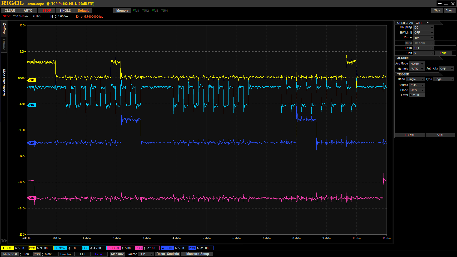
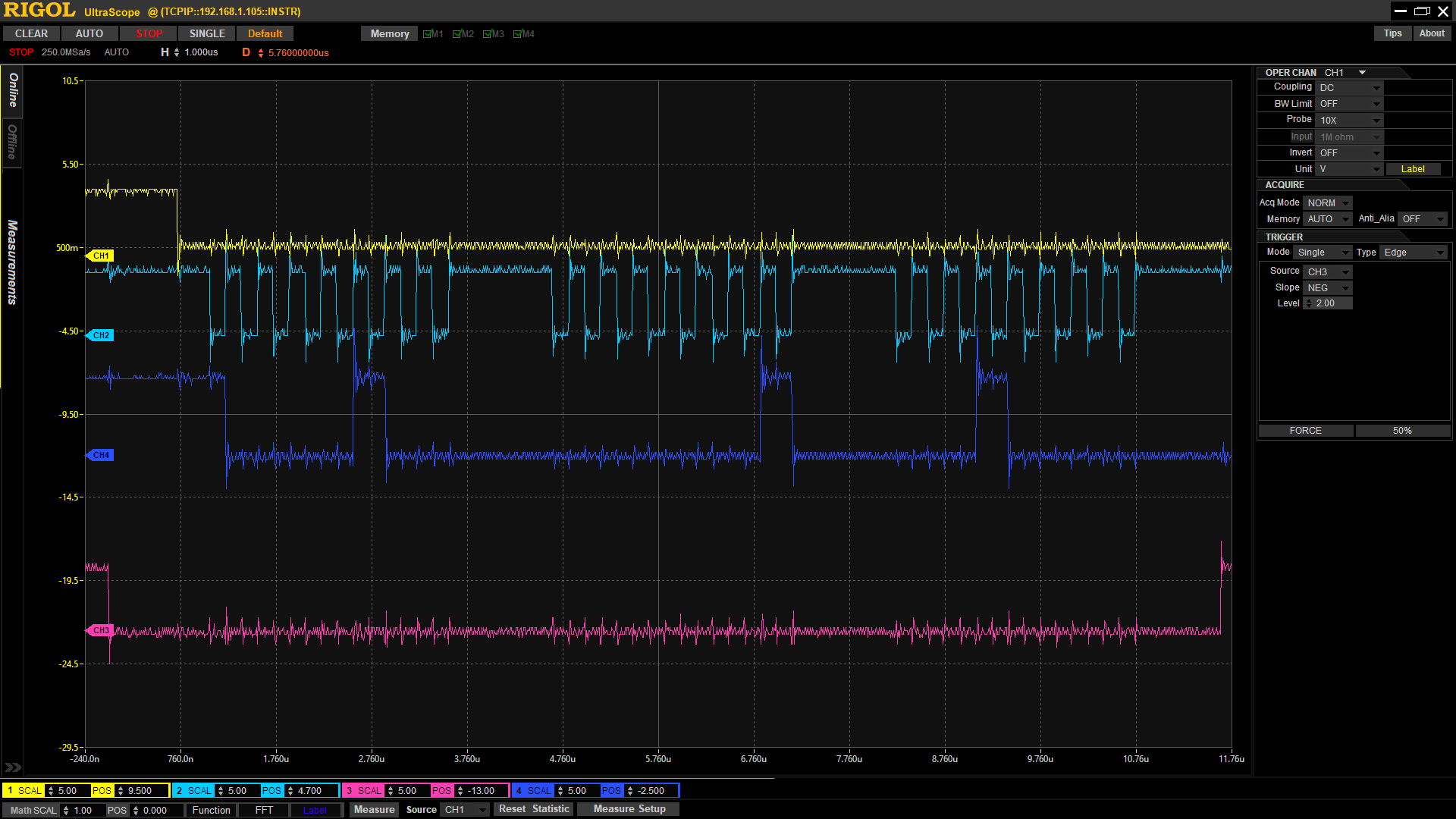
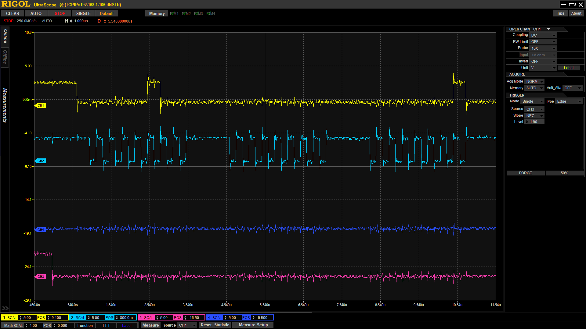
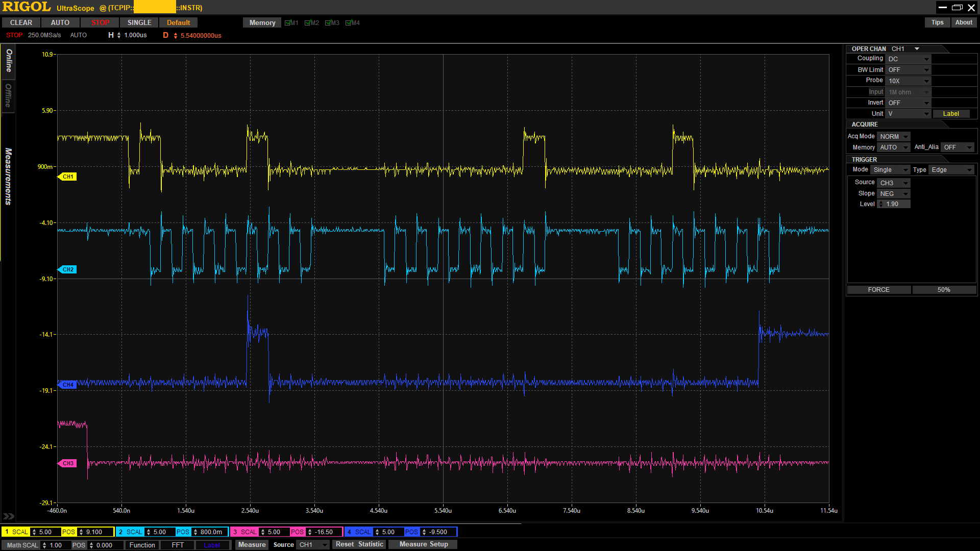
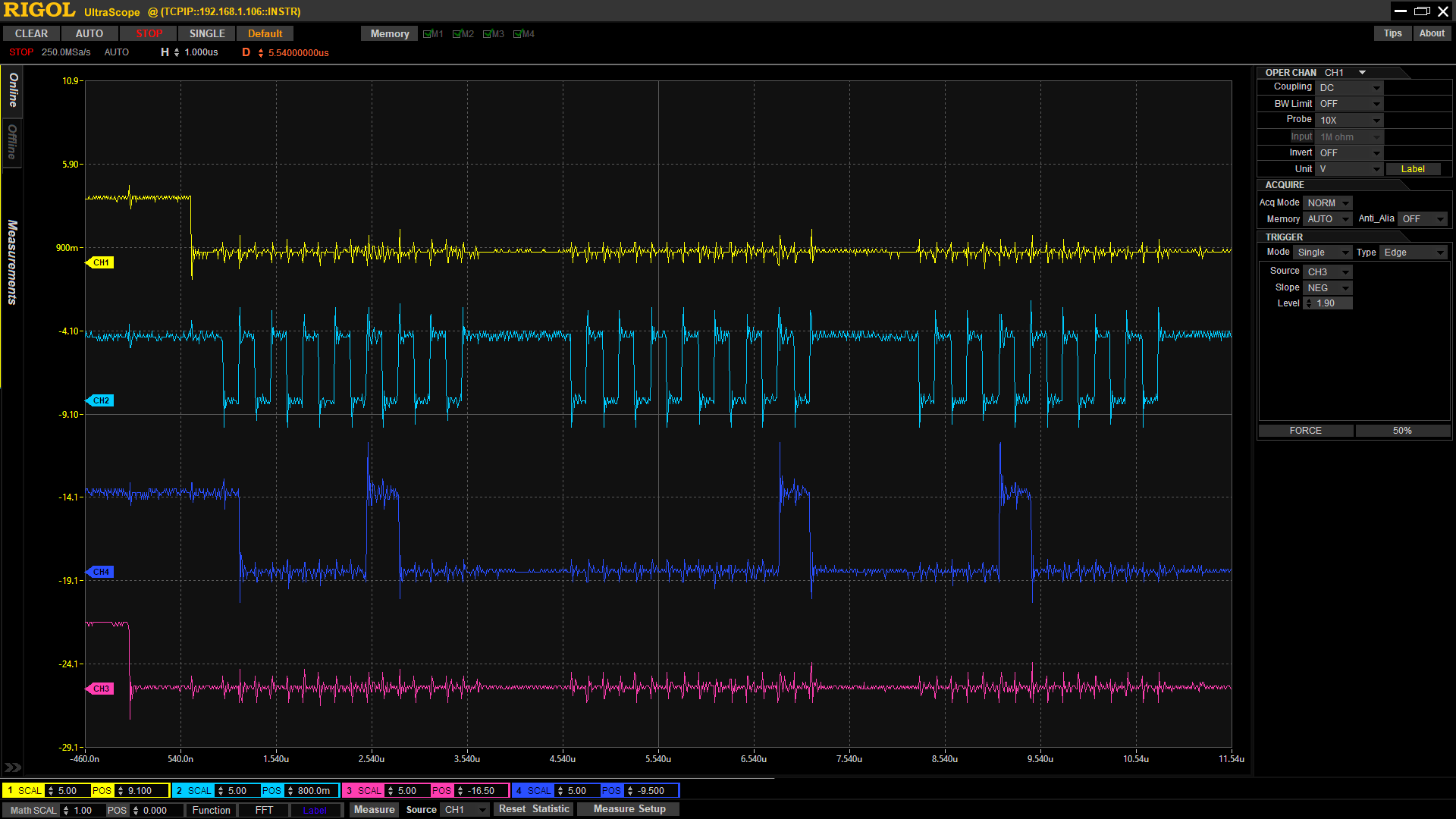
All attempts to read from the device (e.g., status reg=0x0B or POR config reg=0x2) after power reset shows that the device is still in the daisy chain mode. (MISO is echo of last command delayed by 24 bit; and user bit is also 0). I also tried reset the device via register (reg=0x1; data=0x0001) at the startup.

Does the device defaults to  daisy chain mode when BBC is not enabled/configured (via 0x06 and 0x07)? or is there some other issues?

[BBC is disabled for now since VPOS and VNEG of the BBC will be used to power a analog switch (has 3.3V SPI) - not wired at the moment].

Note: I have been testing DAC8775 using the EVAL board, and noticed that I had to replace NOP=[0x00,0x00,0x00] with [0xFF,0xFF,0xFF] in the read command; testing with both MSP432 and Python at the test points of the EVAL board and was working. I tried both 0x00 and 0FF with DAC8771 but nothing works.

Thanks for your help.

  • Lasto,

    Please bear with us as most of the team is off for the Christmas holiday. You can expect a reply sometime next week.

  • Kevin,

    Thank you. No rush at all. Please take your time.

    Happy Holidays!

  • Hi Lasto,

    Sorry for the delay.

    Ultimately, I think you are just seeing the expected behavior of the device. Note that in figure 2 of the PDS we show that the readback data is always seen in the next command, and we use an example of an NOP being used.  

      This does not mean that daisy-chain mode is still active.  Enabling daisy-chain mode basically tells the device to continuously clock out the data after the first 24bits are shifted.  For example, if you had two devices in daisy-chain configuration and you clocked in 48 bits of data, the first DAC would latch the most-significant 24 bits and the second DAC would latch the least-significant 24 bits.  If you left the hardware the same and disabled daisy-chain mode and clocked in the same 48-bits, neither device would latch any data, as the they would see the frame as an invalid length.

    Thanks,

    Paul

  • Hello Paul,

    No problem.

    My apologies as I seem to have caused a confusion here. The key issue for me is that I can't read back data from the device registers (in the firmware). So, I started to look into the SPI signals.

    My issue is that my "Read Command" is reproduced as "Readback Data"  while sending the NOP commend in Figure 2 of the PDS.

    For example, if I set a register (status reg=0x0B or POR config reg=0x2 or user-bit) and try to read it back in the firmware I get the value of the "Read Command" command. I had no problem reading registers from the DAC8775-EVAL with same firmware (sending SPI commands via test points).

    I'm not sure but I believe that I have seen this behavior on DAC8775-EVAL GUI when it was out-of-box, i.e., if not all registers are configured (I had to fiddle with GUI settings to be able to read values from registers - e.g., status reg=0x0B).

    I agree with your note "Note that in figure 2 of the PDS we show that the readback data is always seen in the next command" But, I assume that you're referring to the previous "NOP" command showing as "GARBAGE" segment on SDO in Figure 2  of the PDS. 

    Please let me know if you'd need further information or clarification.

    Best regards.

  • Hi Lasto,

    To clarify, when you do the following:

    1. Write (0x040001) - write value 0x0001 to register 0x04

    2. Write (0x84wxyz) - issue a read command for register 0x04, where wxyz are "don't care bits"

    3. Write (0x000000) - issue a NOP command, the readback data should be present on SDO during this command.

    Are you saying in your post that during step 3, you just see the echo of the 0x84wxyz command rather than the expected "0x840001" (read command but with valid data)?

    Thanks,

    Paul

  • Hi Paul,

    Yes.

    I attached the SPI traces for the above three commands (Yellow=MOSI, Light Blue=CLK, Dark Blue=MISO, Red=CS all at 5V per division)

    [Note I invoked select BBC0 and Ch0 before issuing these write commands to ensure that "disable daisy chain" flag is set as bit 4 of register 0x03 per the PDS]. There is no supply going to the BBC at the moment.

    Thanks for your help. Please let me know if you need any additional information.

  • Hi Lasto,

    What value exactly are you writing to the register 0x03? Could you be enabling the CRC? That might just be causing the SDO pin to echo the response because no other command would be valid.

    Thanks,

    Paul

  • The that I send to 0x03 is 0x0030. The SPI trace is shown below (apology for resolution). The function call is also listed below.

    Thanks for your help. Please let me know if you'd need further data or tests.

     register = 0x03 and data=0x0030 

    void _dac_select_channel(uint8_t ch){  // ch={0,1,2,3}
    
        uint8_t first_ch_bit = 5;  //  for multi-channel DAC, the ch bits are {5,6,7,8}
        uint8_t disable_daisy_chain=1;
        uint8_t dsdo_bit = 4;
    
        uint8_t sel_ch = DAC_MULTI_CHANNEL? ch:0;
        if (sel_ch<DAC_CHANNEL_COUNT){
            uint8_t data[] = {0x00, 0x00};
            uint16_t dec = 1 << (first_ch_bit+sel_ch);
            if(disable_daisy_chain)
                dec |= 1 << dsdo_bit;
            uint8_t mask = 0xFF;
            uint8_t msb = (dec >> SSI_DATA_WIDTH) & mask;
            uint8_t lsb  = dec & mask;
            _spi_dac_write(DAC_CHANNEL_SEL_REG, msb, lsb);
        }
        // else invalid channel
    }

  • Any idea why the image is low resolution? Are you communicating at high frequency? 

    So after re-reading this thread, I think we may be on the wrong path.  This device only operates in daisy-chain mode, or the SDO pin is disabled.  There is no "disable daisy-chain" feature.  Though I admit that the wording for the DSDO bit is confusing.

    Let's try something.  Skip all configurations in your code.  Do not write to config register 0x03.  Just power on the device, and issue these three commands:

    1. Write (0x040001) - write value 0x0001 to register 0x04

    2. Write (0x84wxyz) - issue a read command for register 0x04, where wxyz are "don't care bits"

    3. Write (0x000000) - issue a NOP command, the readback data should be present on SDO during this command.

    You should see a read back.  

    I am concerned that when you write to 0x03, something is going wrong.  Given the noise scopeshot, I am wondering if the data is being mislatched, and you are actually setting the CREN bit.  This would enable the CRC and all other commands would be rejected by the device, though the device would still echo the rejected data on the next command.  In addition, if you were writing to 0x03 correctly, the SDO pin would be high-z and you would not see any response.

    Please give that a test.

    thanks,

    Paul

  • Hi Paul,

    I did reset HW Reset by taking pin 44 low (which is connected to 3.3V via 1K Ohm). Then executed the three commands.

    I included the code for the clock settings below (traces are 1us/div). I'm assuming the clock Polarity and Phase are OK. [The low resolution of the previous snapshot was due to settings of the desktop S/W]

    Please note that SPI coming from MSP432 via TI digital isolators are 3.3V, while DSO is 5V since I'm using internal VDD. 

    I also tried S/W reset and waiting for seconds before re-running the three commands - same result.

    Thanks very much for your help. Please let me know if you need additional tests.

    1. Write (0x040001) - write value 0x0001 to register 0x04

    Write (0x840110) 

    Write (0x000000) 

    Clock Settings

    g_systemClock = SysCtlClockFreqSet((SYSCTL_XTAL_25MHZ |
                                               SYSCTL_OSC_MAIN |
                                               SYSCTL_USE_PLL |
                                               SYSCTL_CFG_VCO_480), 120000000);
    // default ssi to support DAC after initialization
         MAP_SSIConfigSetExpClk(SSI2_BASE, g_systemClock, DAC_SPI_MODE,
                                    SSI_MODE_MASTER, (g_systemClock/40), SSI_DATA_WIDTH);

  • Hi Paul,

    I apologize since my last post was missing the conclusions of the test, which "hardware resetting did not make any difference, the daisy chain is still active".

    Thanks

  • Hi Lasto,

    I just tried this with my DAC8775 EVM, and I did not have any trouble.  I verified that the nature of the NOP does not matter (0x000000 or 0xFFFFFF), you could also just send the read command again and still works.

    I will order the DAC8771 EVM as well just to be sure.

    As I am running low on ideas, let's just clarify some stuff just to make sure we are not missing anything:

    1. Are there any other devices on this SPI bus?

    2. On your scopeshots, I see some significant ringing on the clock edges.  I have seen these cause problems in the past, especially if this is a "fly-wired" setup.  The scope probes usually improves this, so they could be even worse when you have the probes disconnected.  How do you have this board wired? would it be possible to add some series resistance before the device pins, and small capacitor (<100pF).

    3. Can you share a schematic?

    4. Does anything change if you slow down the clock?

  • Hi Paul,

    I attached 3 files (2 schematics of the DAC8771 and digital isolators; and an overview of the 6-layer board). Answers are listed below:

    1. Are there any other devices on this SPI bus?

    Not during this testing, only DAC8771. There were ADC and Analog Switch (I removed the switch and disconnected the MISO of the ADS). The MOSI, CLK and are still shared with the ADC only (but separate CS). I marked these changes with two Red 'X' in the attached schematic of the digital isolators (schematic_ISO7740DBQ_ISO7741DBQ_for_MSP432E_DAC_SPI_Isolation.pdf)

    2. The test points are connected to the probes via "Fly Wires" and alligator clips. I have zero resistors that can be replaced with 33 Ohm for MOSI, CLK and CS lines (but not for the MISO).

    3. Shared 3 files; please let me know if you'd need further information.

    4. I'll slow the clock and retest and keep you posted.

    Thanks again.

    DAC8771 schematic

    schematic_DAC8771.pdf

    Schematic of the SPI lines Digital Isolators

    schematic_ISO7740DBQ_ISO7741DBQ_for_MSP432E_DAC_SPI_Isolation.pdf

    Layout Overview

    Layout_Overview.pdf

  • Hi Paul,

    Regarding clock speed:

    4. Does anything change if you slow down the clock? No. (slowed clock by factors 2,4, and 8)

    Thanks

  • Hi Lasto,

    Are you able to configure the DAC at all? For example, are you able to get the voltage output to change just by writing to the device?  Could the device be in some reset state where the interface is just in a dummy mode?  Can you verify all the supply voltages?

    Thanks,

    Paul

  • Hi Paul,

    I never tried to enable the BBC arms on the DAC8771 yet. In other words, I'm currently using SPI communications while BBC disabled (hence there will be channel faults)

    [As I mentioned in my original post, I think reading/writing registers via TI GUI (second tab) was also an issue on the out-of-the-box DAC8775 EVAL, until I enabled the BBC and selected channel.]

    I measured the supply, BBC and Vout voltages:

    * AVDD/PVDD =12.1V (my DAC8775 EVAL is fully functional down to AVDD=8.5V);

    * BBC - VPOS=0.7V and VNEG=-150mV;  since BBC is not enabled  (i.e., never configured bits 1:0 of reg 0x07 on the DAC8771) 

    * Vout = < 0.5 mV (register 0x04 = 0x0001 per your instructions, 0x05 is at reset=0x0000)

    Here's how I typically configure BBC (on DAC8775-EVAL is working fine with SPI from MSP432 through test points)

    void dac_enable_all_bbc(){
        uint8_t ch=0;
        uint8_t output_range_data=0x0;
        for(ch=0;ch<DAC_CHANNEL_COUNT;ch++){
            _dac_select_buck_boost_converter(ch);
            _dac_select_channel(ch);
            output_range_data = dac_get_ch_output_range(ch);
            if(output_range_data < 4 || (output_range_data > 7 && output_range_data < 12))
                _dac_set_buck_boost_converter_configuration(0x01, 0x08, 0x07, 0x03);
            else{ // if(output_range_data > 3 && (output_range_data <8) || output_range_data >= 12))
                _dac_set_buck_boost_converter_configuration(0x00, 0x08, 0x07, 0x03);
            }
        }
        _spi_dac_flush();
    }

    Please let me know if you need any tests or data.

    Thanks

  • Hi Lasto,

    Can you try enabling the DC/DC converters on the DAC8771? I would like to have some confidence that we are able to write to the DAC successfully.   If we cannot write to the DAC, then I suspect we have some schematic issue where the device is in some POR state, where the digital interface is just echoing the input.

  • Hi Paul,

    I tried to enable the DC/DC converter for channel 0 to clamp to +/-15V (reg=0x07, data=0x061F) but it did not work. 

    So, it seems that I can't write to the registers. Also, I assume that we verified that disabling DC/DC converter (writing 00 to 0x07 1:0 bits) does not impact SPI communications. 

    I sent the schematic of DAC8771 and ISO7741DBQ digital isolator above. I checked the reset voltage at pin 44 and it is high (3.25V), also pin 45 (Alarm) is high (3.21V). I'm still writing 1 to DSDO bit when selecting channel 0.

    Please let me know if you need additional information, tests or schematic.

    Thanks

  • Hi Paul,

    There are other two possibilities, (1) my firmware might be causing an issue (sequence of calls or timing); (2) DAC and Isolators power supplies sequence issue.

    Firmware: I used an identical firmware to communicate with DAC8775EVM, where SPI commands were through test points (not via SM-USB-DIG). Although I had no issues writing and reading from registers and DAC8775 performed flawlessly; I had to reset and enable BBC at the startup in order to be able to read status and other registers. May be I'm not following the correct startup sequence, but everything was working fine afterwards.

    Power Supply: I have two 3.3V (LDO) power supplies, one (digital) is feeding the Isolators and the other (analog) is connected to ~Reset and ~Alarm. The DAC AVDD comes from TI LP38798SD buck.

    Thanks

  • Correction TI LP38798 is an LDO.

  • Hi Lasto,

    There are a couple steps to enabling the DC/DC converter.  How about we try just to enable the reference. 

    Try resetting the device, and just writing to the REFEN bit (register 0x02 value 0x0010), you should be able to measure the voltage on the REFOUT/IN pin.

    In addition, can you verify that when you power the device, you see about 3.4V on VPOS?

  • Hi Paul,

    It seems that, as you suggested, the Reset pin was not kept in low state for some reason (could have been a void contact). Now I can read the status register and it passes the reading test that you suggested above.

    The Reference voltage is 5V now.

    But the VPOS is -0.5V not 3.4V (I enabled both arms of DC/DC converter to clamp to +/-15V, but I disabled the channel output). VNEG= -1.3V.

    Are you suggesting that VPOS should be 3.4V when DC/DC is disabled?

    Thanks. 

  • My understanding is that VPOS should be ~3.4V assuming PVDD and AVDD are supplied.  What happens when you enable the DC/DC?

  • Hi Paul,

    Here are the values of VPOS and VNEG with DC/DC Disabled

    * DC/DC Disabled - VPOS=0.7V and VNEG=-150mV;  when BBC is not enabled  (i.e., bits 1:0 of reg 0x07 to 00)

    * DC/DC Enabled - VPOS=-475mV and VNEG=-1.29V;  when BBC is enabled  (i.e., bits 1:0 of reg 0x07 to 11)

    Please let me know if we need to get a tarce of the DC/DC signals (e.g., Voltage across Lp to Ln).

    Note: Although the schematic is identical to that of EVM, I'm connected VPOS and VNEG as a supply to two other devices via bypass capacitors (one is analog switch which is currently removed from the board and an OpAmp/Buffer). The total bypass capacitance is 10uF per device for each rail (VPOS and VNEG). If necessary I can send you the schematics of the DAC and relevant devices, via a PM if you send me an E2E invite. 

    As in the reference design (EVM), the VPOS and VNEG are also connected across the BAV99-7-F at the output port.

    Thanks

  • Here sre the register settings based on SPI traces:

    The status register is 0x1740 indicating DC/DC PG=0 (not good); the expected value for 0x17C0 (since I'm setting the UBT to 1)

    The SPI is reading back all registers of the device correctly. The reference voltage is 5.02V.

    Register 0x07 is set to 0x061C when disabling DC/DC (and is set to 0x061F when DC/DC is disabled)

    Register 0x06 is set to 0x0001 before setting reg 0x07

    Thanks!

  • Hi Lasto,

    Can you email your schematic to frost@ti.com?

    Thanks,

    Paul

  • Hi Lasto,

    Let's mark this thread as resolved and I can support the DCDC issue over email.  I believe it is a minor schematic error so not relevant to other users.

    Thanks,

    Paul

  • Hi Paul,

    I fully agree, as you suggested it was the Reset pin contact that caused the device to fail moving data from the shift register to device registers.

    Thanks very much for your help.