This thread has been locked.

If you have a related question, please click the "Ask a related question" button in the top right corner. The newly created question will be automatically linked to this question.

ADS8668: Design Review

Part Number: ADS8668
Other Parts Discussed in Thread: DAC7760, ADS8688

Hello,

I posted a schematic several months ago and implemented the feedback I received. However, the design is still causing issues. I have combed through the data sheet and other examples and cannot find the problem. 

Currently the with inputs floated, the read back on SPI is always high and when I meter the front end of the input channels (in front of and behind the filter), there is a strange 2.005V signal that appears. The chip is laid out on a PCB following the guidelines spelled out in the datasheet. 

My code has been tested using the ADS8668EVM and functions perfectly using only the 4 SPI signals (so it is most likely not a software issue). 

Is there something I'm overlooking?

Any help would be appreciated. 

Thanks!

  • Note: all grounds are tied together both on and off the PCB

  • Hi Matt,

    I did not see any issue in your schematic, can you please check and provide following information?

    1. Measure the voltage on Pin 5 (REFIO) and Pin 7 (REFCAP)?

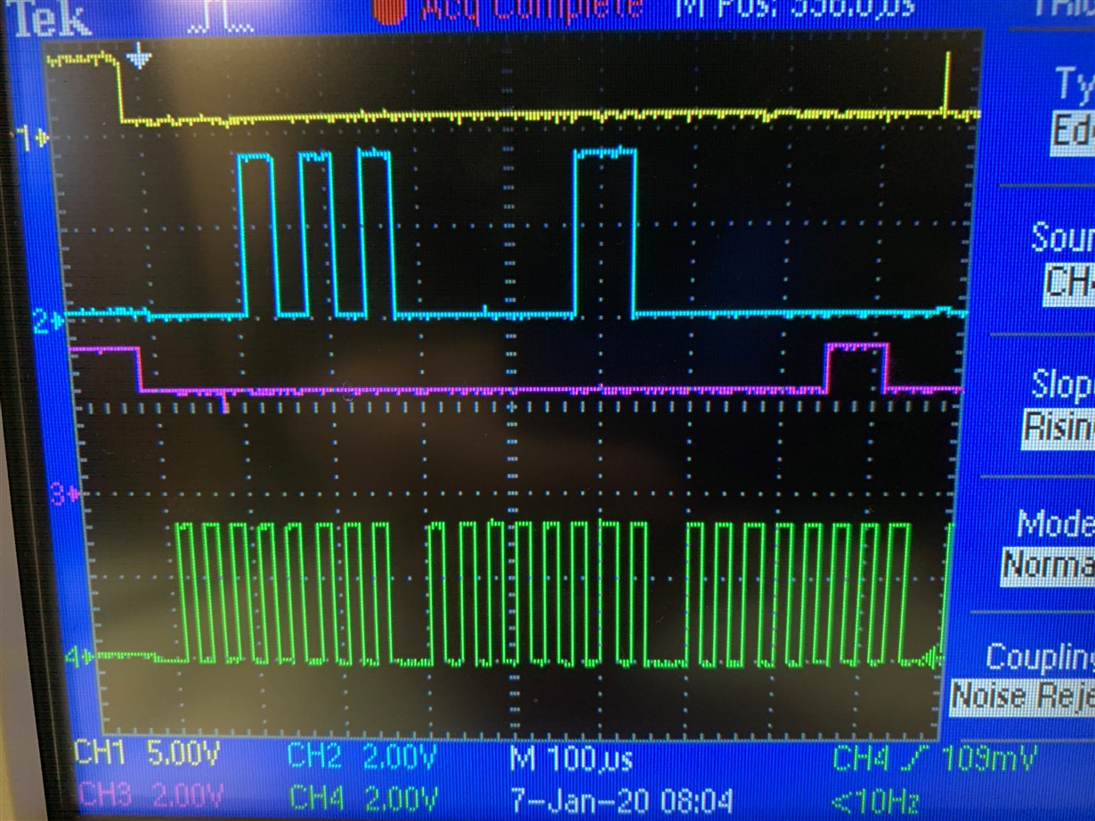
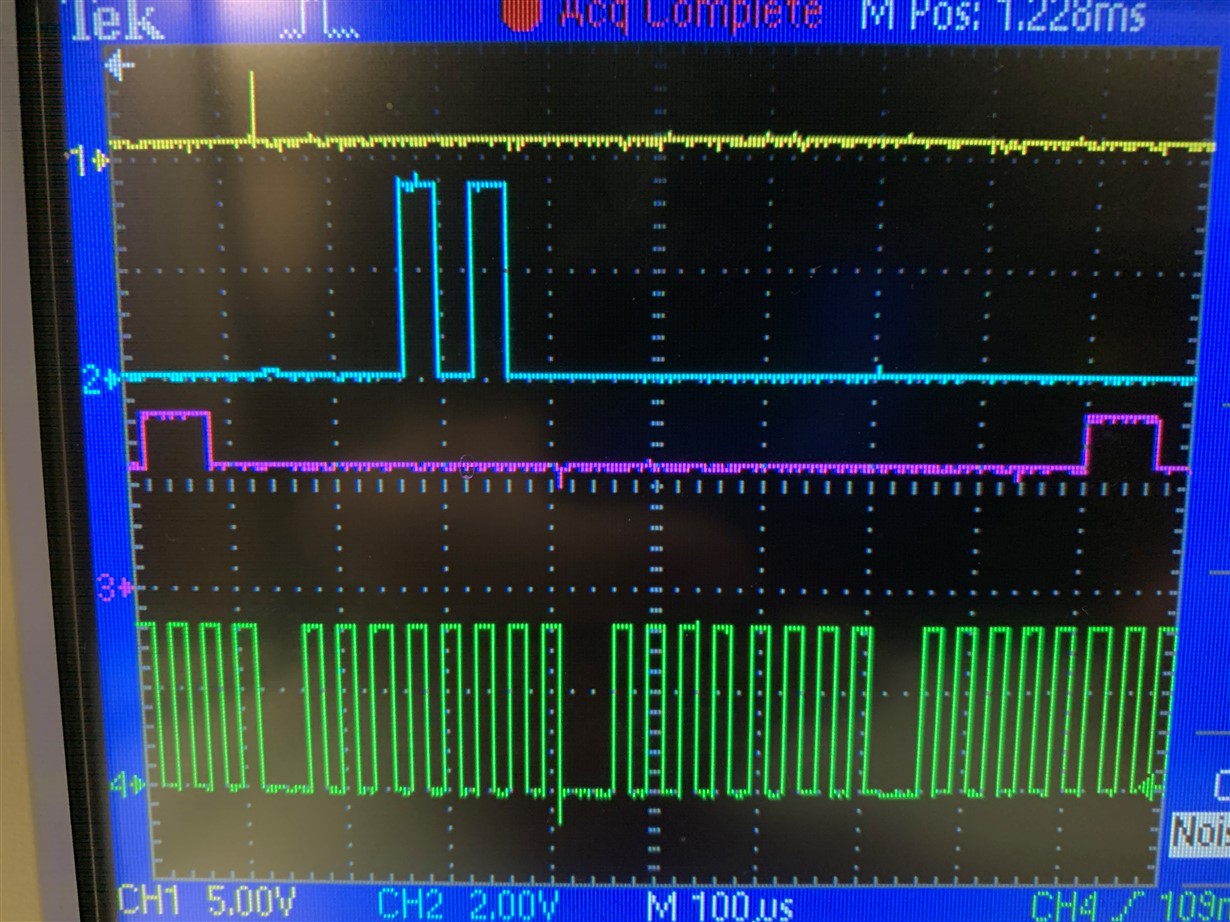
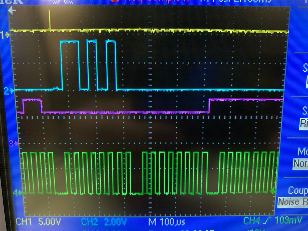
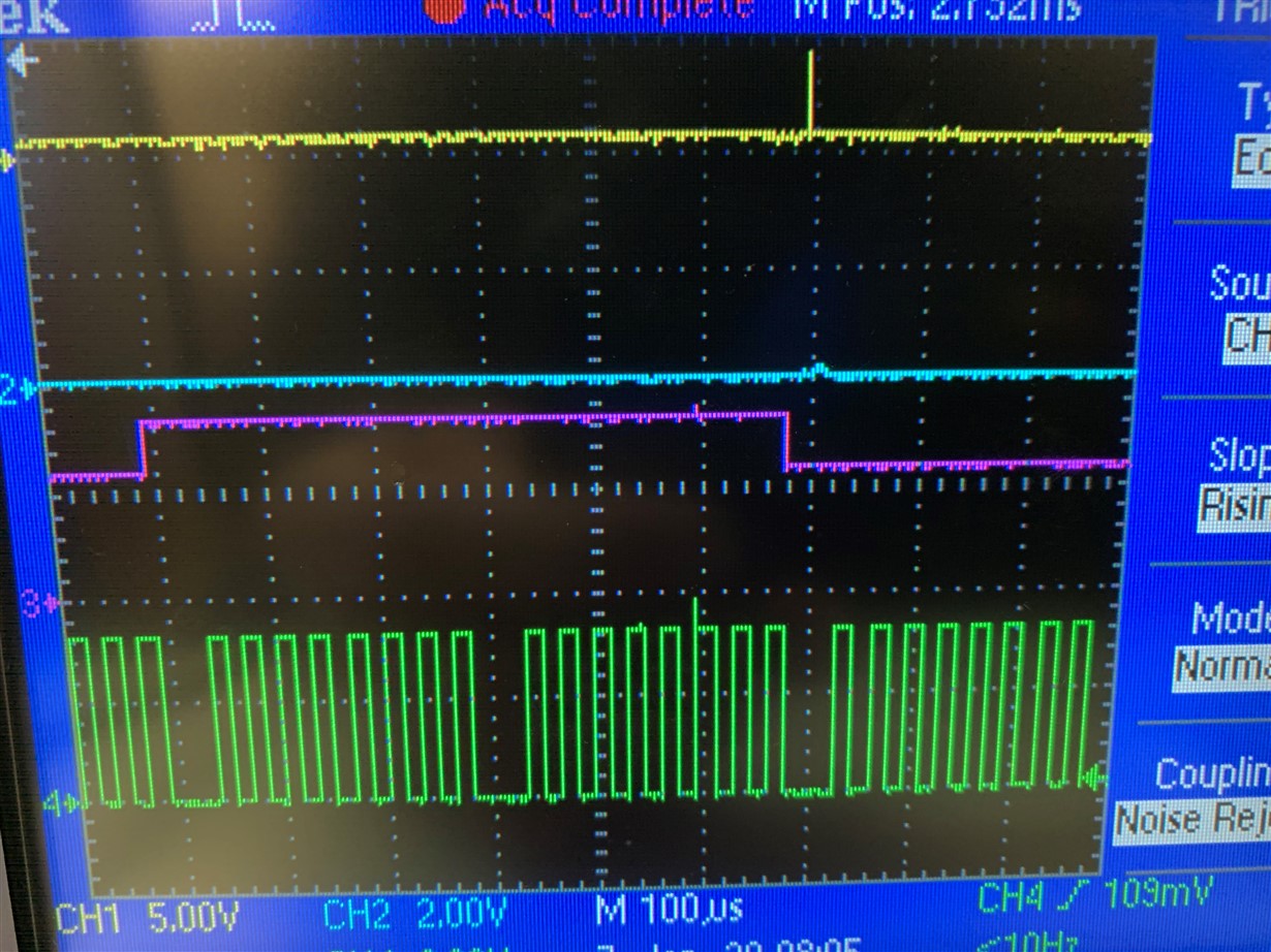
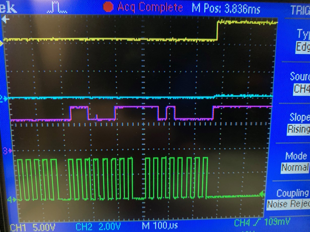
    2. Capture timing (/CS,SCLK,SDO and SDI) with an oscilloscope

    3. Where are you connecting AGND and DGND on your physical pcb board?

    Regards,

    Dale

  • Dale,

    Thanks for the reply.

    Pin 5 (REFIO) measures: 4.096 V

    Pin 7 (REFCAP) measures: 4.096 V

    AGND and DGND are connected near the header input of the PCB (approximately 3in from where the ADC is located then again off board at the din rail connections

    Scope Images: I apologize they are only photos from my phone, the screen capture on my scope is currently out of order

    Signals are as follows:

    1. CS

    2. MOSI

    3. MISO

    4. SCLK

  • I am applying a 2V signal to channel 5 of the ADC that has been verified on the front end of the filter.

  • Now that I have looked closer, I believe I have found the error in the MISO signal. Some insight that may be helpful:

    on this board is also a functional DAC7760 circuit which I believe is holding the MISO signal high.

    They are connected to the same SPI signals with separate CS signals

    Here is the schematic for that circuit if you can see any reason it would be pinning that signal high. 

  • Hi Matt,

    Thanks for information. Firstly, I suggest to remove/disable the DAC or disconnect the MISO from the DAC, then check ADC's code and timing again. Secondly, your reference voltage is correct, your screenshots shows different commands to the ADC, for example, the 3rd screenshot shows that D400h is sent to the ADC to select CH5 channel, other screenshots shows you are accessing program registers which are not related to channel selection and conversion. Please confirm. Finally, you are communicating the ADC with 4x8 clocks, this can lead to a longer tPL_CK than 0.6 tSCLK, I can not verify with limit resource now, however it will be good to use continuous 32 SCLKs or 2x16 SCLKs for SPI communication.

    Regards,

    Dale

  • Hey Dale,

    Thanks for the reply.

    I floated the MISO pin from the DAC at the front end of the isolator and the MISO voltage remains at 3.3V even when a signal is sent by the ADC on that line.

    Several of the photos are overlapped so here is the current registers being sent.

    send_data[0]=0x15;
    send_data[1]=0x06;
    send_data[2]=0x00;
    bcm2835_spi_transfern(send_data,3);//write to the register at 0a value 06 range select register to 1.25*vref


    send_data[0]=0x14;
    send_data[1]=0x00;
    send_data[2]=0x00;
    send_data[3]=0x00;
    bcm2835_spi_transfern(send_data,3);//read the register at 0a.


    send_data[0]=0xd4;
    send_data[1]=0x00;
    send_data[2]=0x00;
    send_data[3]=0x00;
    bcm2835_spi_transfern(send_data,4);//read analog input at 5

    This has been run on the ADS8668EVM and returns an accurate value but could it be an issue with initialization? 

    Thanks!

  • Hi Matt,

    I apologized for missing your post. I re-checked the information and the question from you, you observed a "strange" 2.005V signal on analog input when the input is floating. Actually, this is a right and normal phenomenon for this ADC. ADS8688 integrates an analog front-end (AFE,PGA) on every channel, there is an internal bias voltage signal (~2V for +/-1.25Vref input range, ~2.25V for +/-2.5Vref input range, see Input Leakage Current information in page 7 of ADS8688 datasheet) provided to this AFE as shown in below block diagram, the input signal is biased to the appropriate common-mode voltage level for proper operation of internal ADC core. When an available input signal is shown up on ADC input, the input signal will dominate it. When the input is floating and no any signal, the bias voltage will be observed, this is why 2.005V was observed by you since your were using +/-1.25Vref input range. Notice that the converted voltage/code may be different if a pull-down resistor is used before the external LPF filter. Since these ADCs support true bipolar input signals with a single +5V power supply, the internal biasing cannot be done to provide a zero offset at ADC output when the inputs are left floating. One of the advantages of this input stage is that it offers a 1-MOhm constant resistive input impedance. This makes the inputs relatively easy to drive (i most cases) without additional driver amplifiers or buffers.


    Please let me know if you have other question.

    Thanks&regards,

    Dale