A related question is a question created from another question. When the related question is created, it will be automatically linked to the original question.
If you have a related question, please click the "Ask a related question" button in the top right corner. The newly created question will be automatically linked to this question.
How is the output wrong? Is it not updating at all or are you seeing an incorrect value as intended? The data is latched on the rising edge of CLK, is that what you are intending?
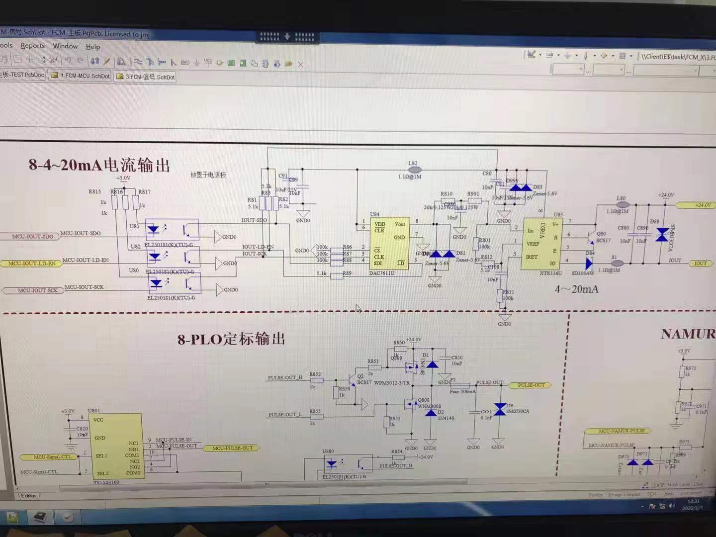
I have tried to some datas, they are wrong,001(1mV),002(11mV),004(47mV),008(190),010(765mV),020(3064mV),040(0mV),0080(0mV),100(0mV),200(0mV),400(0mV),800(0mV),030(3831mV),038(4022mV),03C(4070mV),03E(4082mV),03F(4086mV)
That transition is acceptable, assuming the data is valid during the transition. 100kΩ on the input pins is a bit high, as our IIL and IIH specification is 10µA max. Can you also verify if your isolation stage is inverting your data? Also, please verify the voltage on VDD is correct. What does LD look like after the data is written?
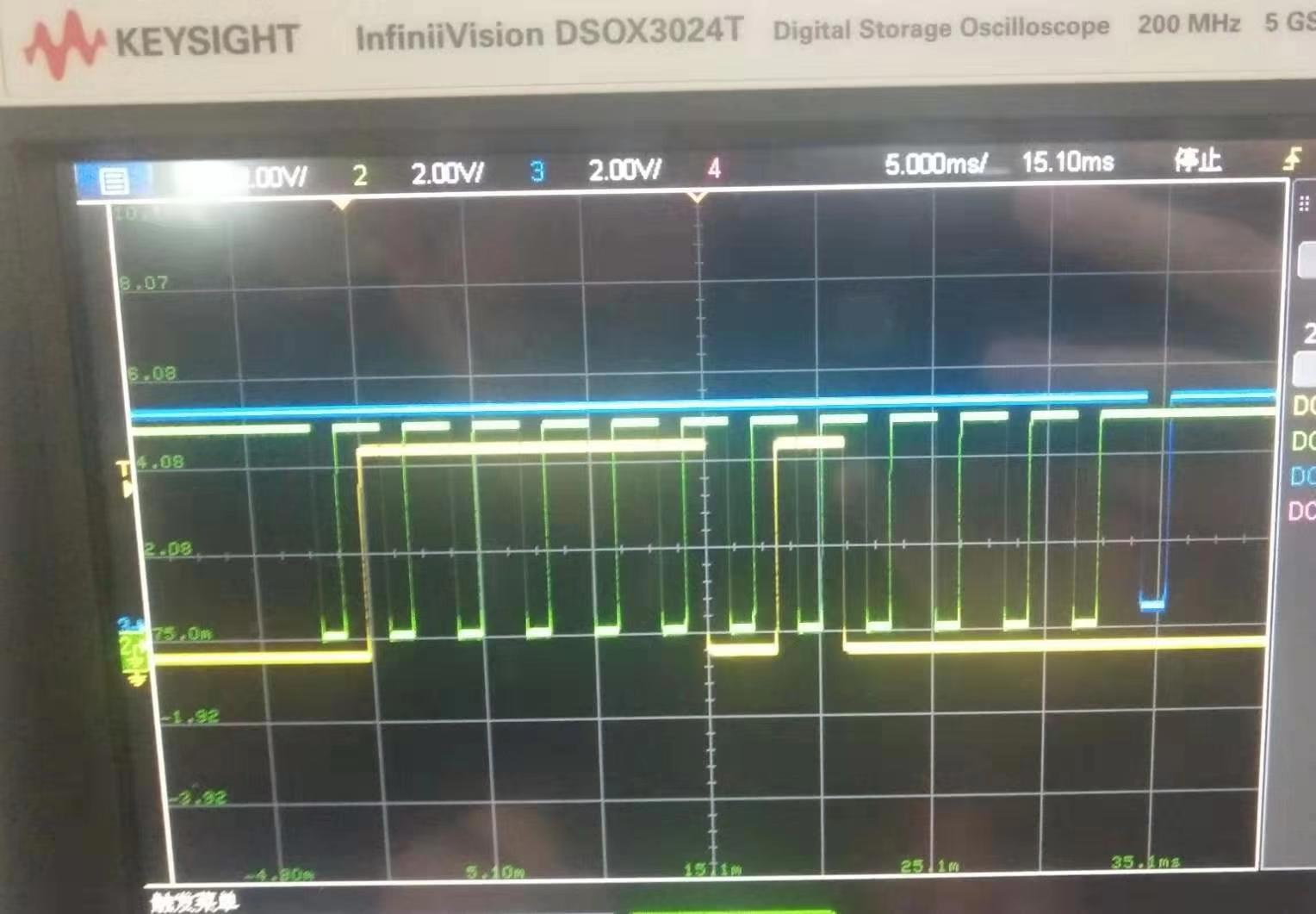
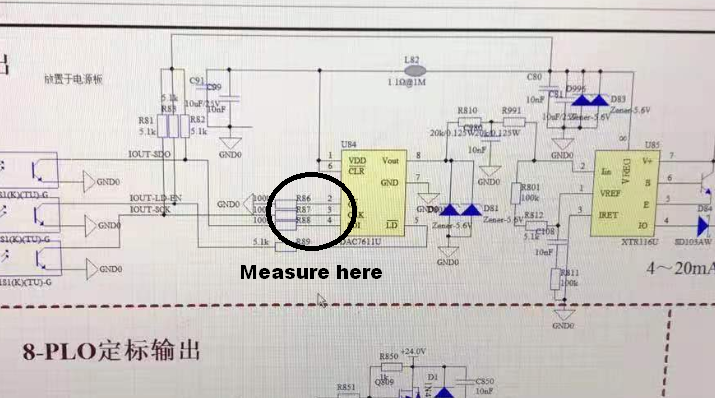
1. I do think the rise and fall time alone is the problem, but rather that the edge timing is causing the data to be misformatted. The isolator's datasheet shows that the tRISE and tFALL time for ~5kΩ is ~100µs. I am concerned that the data as shown in the first image is not valid with those edge transitions. Please collect another image, similar to the one below but measured directly at the DAC pins.
"I am concerned that the data as shown in the first image is not valid with those edge transitions."
reply: I'm sure the data is valid with those edge transitions,because the data is Stable ,"0"(0V)or “1”(5V) ,when the clk changed from 0 to 1 and the data keep enough time accordind with the datasheet .
"Please collect another image, similar to the one below but measured directly at the DAC pins."
reply:The waves of you see all the pictures are measured directly at the DAC pins.
rely:we have tried “0b000000111111” was 63mV,when R81=2K. "The data format is Straight Binary and is loaded MSB-first into the shift registers." It means we should transmit "0" at 1st clk,“0” at 2nd clk ,“0” at 3rd clk, “0” at 4th clk,,,,,you can see Yuan's pictures.
Something to consider is that there are critical digital input voltages that result in the DAC7611 drawing more current.
My suspicion is that the slower ramp rates when using 5.6kΩ resistors result in the VREG output of the XTR116 to collapse or drop enough that the VIH and VIL levels change momentarily, this could cause the device to latch the incorrect data, or potentially reset the part during the transmission.
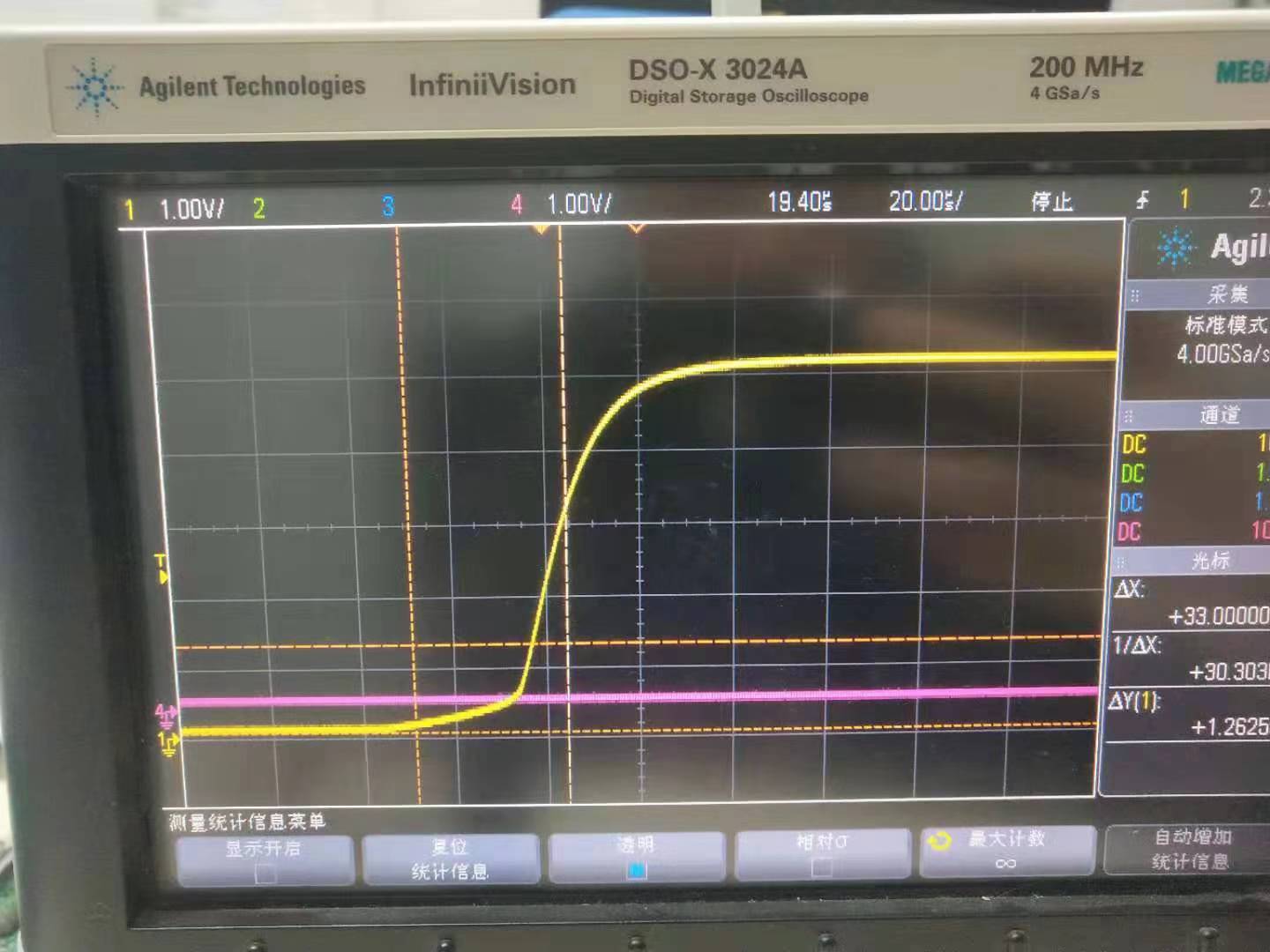
Note the current sourcing capability of the VREG output is pretty limited. With a typical short circuit current of 12mA. This plot in the XTR datasheet shows the VREG output drop with just a few mA of current.
Using 2kΩ means that the time period where the current is high is shorter, so the supply might not be collapsing enough to cause a problem. There is a balance that must be found as the 2kΩ resistors also take from the total current budget.
I suggest two experiments:
1. Monitor the VREG output during the communication with both 2kΩ and 5.6kΩ. This will give us an idea of how much the supply has collapsed.
2. Try sourcing VDD externally. If the supply is approximately the same voltage as VREG, then they can even be connected in parallel. If communication using the 5.6kΩ works with an external supply, then we have high confidence that the supply drop is the problem.
I have not been able to reproduce this. I suspect that the very slow edges are causing this high-current state and that is causing a reset. Are you able to use the lower resistance values in the application? If that impacts the current budget too much, could they implement a simple digital buffer to remove the slow edges from the DAC?