This thread has been locked.

If you have a related question, please click the "Ask a related question" button in the top right corner. The newly created question will be automatically linked to this question.

ADC12DJ3200: JESD204B configurations

Part Number: ADC12DJ3200

Hello, 

I start looking into the "slac748_adc12dj3200_A10fpga_jesd204b_from_TI", the source code and user guide etc. 

I noticed that the JESD204B configuration seems different between user guide and the source files, in which the source file are restored with Quartus Prime Pro version 16.1.

For example, it shows K= 4 in the user guide for configuring ADC but the K = 32 in "altera_jesd2041_.... v", see below. The values below matched with QSYS setting. 

altera_jesd2041_altera_jesd204_161_kzbcg4i #(
.DEVICE_FAMILY ("Arria 10"),
.SUBCLASSV (1),
.PCS_CONFIG ("JESD_PCS_CFG2"),
.L (8),
.M (4),
.F (1),
.N (16),
.N_PRIME (16),
.S (1),
.K (32),
.SCR (1),
.CS (0),
.CF (0),
.HD (0),
.ECC_EN (1),
.DLB_TEST (0),

My questions are:

Q#1, should K =32 or K=4 be used? Also other parameters if differed. 

Also, in the user guide, it states "In this EVM revision P & N pins of upper four SERDES lanes are swapped, hence Rx lane polarity inversion is implemented in the design to address that." So,

Q#2, which FPGA module or block address it. 

Hope to hear from ASAP.

  • New2Day:

    There may be some flexibility to setting the K value dependent on your HW and FPGA.  Typically this value must be optimized for a given system.  That may explain the difference between a TI set-up with TI capture solution vs other HW and FPGA capture solution.

    The swapping of the pins may be referencing settings in the ini file to invert the proper pins.  I will defer this post to the ADC12DJ3200 expert to confirm and expand on my explanations.

    --RJH

  • Hi,

    #1

    As shown in my post(highlighted), besides K, N/N', S and F are not same neither.

    I'm guessing it's due to use version 16.1 Quartus Prime Pro and Arraia 10 SoC FPGA so IP core were updated. 

    So I like to confirm all parameters should be matched with values set inside ADC device. 

    #2

    I have put following signals onto Signal Tap and observations:

    rx_link_clk_rstn   = LOW

    pll_locked = HIGH

    serdes_data_in = all '0'

    serdes_data_valid = all '0'

    rx_ready = HIGH

    rx_is_lockedtodata = LOW

    in which, rx_link_clk_rstn is LOW is due to rx_is_lockedtodata are LOW. rx_is_lockedtodata are LOW may be due to serdes_data_in not BCBDBC. . ..

    I like to get your opinion why serdes_data_in are not BCBCBC. . and or rx_is_lockedtodata are LOW. 

    Thank you.


  • Hi,

    I am going to take a look at the design and will let you know by 01/22.

    Regards,

    Neeraj 

  • Thanks a lot. 

    I found and changed the code that set upper lane[7:4] to be non-inverted. 

    For the link-up and aligned issue (rx_is_lockedtodata are LOW), hope to hear from you ASAP. Thank you very much. 

  • Hi,

    Any updates? Hope to hear from you ASAP. Thanks.

  • Hi

    Here are few things I would like you to try.

    1. Make sure the ADC is getting the proper clock and enough current(3A) and is getting programmed properly. You can try to write a value to the ADC and read the value back and make sure it is as expected.

    2. Make sure the SYNC pin from the FPGA routed to ADC SYNCSE pin.

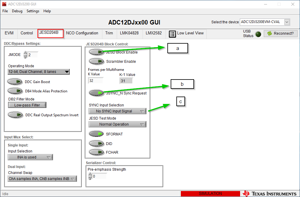
    3. You can force the ADC into CGS mode by doing a software sync. Here are instruction below.

    a. Disable JESD BLOCK by clicking the JESD block enable button.

    b. Click the JSYNC_N sysnc Request.

    c . SYNC input Selection select no SYNC input Signal

    d Enable the JESD block back.

    Regards,
    Neeraj

  • SignalTap.rtfHi,

    I'm not using the EVM but our own board. I'm using the "ARRIA 10 JESD REFERENCE DESIGN" from TI. 

    I have tried all things mentioned above and more:

    1. I have no problem write and read ADC registers and clock is 3GHz @ 3dBm from Sig Gen

    2. Yes, SYNC pin is connected to FPGA and FPGA will issue a SYNC to ADC once the rx_is_lockedtodata signals go HIGH from JESD204B receiver (PHY)

    the problem I'm having is that rx_is_lockedtodata signals didn't go HIGH and there are no "BCBCBC.." on serdes_data_in bus. See attached signal tap screenshot. 

    of cause FPGA won't issue a SYNC and register 0x208 of the ADC is 0x4.

    I'm waiting for the insight or answers or ideas why.  ASAP please. 

    About SYNC by register 0x203 after disable JESD block and then setting  0x204 to 0xA, the register 0x208 changed from 0x4 to to 0x64. 

    However, nothing changed on two signals(buses) mentioned above. 


  • Hi

    It sounds like the FGPA is not getting proper reference clock and hence it is not able to get the lock on serdes) can you please make sure the proper refence clock is getting to the FGPA.

    Regards,

    Neeraj

  • 1. FPGA DEVCLK is 300MHz and ADC sampling clock is 3GHz. SYSREF to both FPGA and ADC are 3GHz/640 while mgmt clock is 100MHz.

    The screenshot of signal Tap attached in last email is running at 300MHz, in which mgmt clock and SYSREF are in it. 

    2. I've also tried recompile the FPGA project to run at lower rate as below but again no luck.

    FPGA DEVCLK = 125MH and ADC is sampling at 1.25GHz

    Thank you.

  • Hi,

    I am going to talk to our firmware team and see if we can solve your issue. In the mean time can you make sure if the ADC eval board is getting 5V and at minimum 3A of current.  

    Regards,

    Neeraj  

  • Hi,

    Can you please share a screenshot of signal tap signals when the CGS mode is forced in the ADC by following the instruction in my previous post?

    Regards,

    Neeraj

  • Hi,

    I finally managed to get the "rx_is_lockedtodata" going HIGH and "serdes_data_valid" to HIGH. 

    The "serdes_data_in" are all x"BCBC..." after changing the K to be 32 (KM1 = 31)

    However "dev_sync_n" is not HIGH and not data output on link layer. 

    I use "ADC12DJxx00_JMODE2.cfg" for setting up the ADC and register 208 is x"4'. 

    Based on the JESD204B protocol, I'm guessing it has something to do with SYSREF vs. ADC sampling clock. 

    Q1:

    Can ADC runs with external clock? Which is independent from SYSREF to the ADC. 

    Q2:

    SYSREF going to FPGA and ADC have same frequency at 3GHZ/640, was it OK? (it meets the formula). 

    4530.signalTap.rtf

    It'll be great appreciated if you have any insights and or suggestions. Hope to hear from ASAP. 

  • Hi,

    Can you please confirm the following.

     The FW is tested at 12Gbps lane rate with reference clock of 300Mhz. As we can see the SYNC is not asserting, Please carry the following Debug steps,


    1.       Arm/Trigger the Signal tap for SYNC rising edge (To understand if SYNC is toggling during capture).

    2.       Probe the following debug signals from the JESD Base IP,

                                                                   i.      jesd204_rx_dlb_errdetect – to detect 8/10B error

                                                                 ii.      jesd204_rx_dlb_disperr – to detect running disparity error

    If the above signals are showing error values, we can understand there is an issue with the signal integrity of the link

    3.       Can you please make sure the SYSREF frequency is an multiple of an LMFC period?

    LMFC Frequency = 37.5 MHz (for JMODE 0/2 with lane rate of 12Gbps)

    Regards,

    Neeraj

  • Hi, 

    Thank you very much for the follow-up. Here are the updates refer to the # in your post:

    1. actually SYNC is toggling after reset, which is go to HIGH and then LOW again, it stays LOW after

    2. no errors, see attached

    3. SYSREF = Fs/640 = 3GHz/640 = 4.6875MHz. 

    About LMFC Frequency, did you mean SYSREF should be 37.5MHZ?

    according to the JESD204B,

    LMFC = Fc/K = Fs/K*S = 3GHz/4*5 = 150MHz,  S= 5, K= 4 when JMODE = 0 or 2

    rx_dlb.rtf

  • Hi,

    So is your issue fixed now?

    Regards,

    Neeraj

  • Not yet, it's strange,  

    #1

    As mentioned, dev_sync_n is toggling after reset. It's from LOW to HIGH for a while and went back to LOW then stays at LOW unless another reset. 

    When it's HIGH, dev_lane_aligned is HIGH too, _rx_link_data seems flowing from ADC while _rx_link_data_valid is HIGH.

    #2

    after dev_sync_n went back to LOW, ADC is sending x"BCBC.." again. 

  • Hi,

    It sounds like you have signal integrity issues. Can you please try the PRBS pattern test or Ramp test pattern and see if you see the signal integrity issues?

    Regards,

    Neeraj

  • I have run transport layer test pattern and ramp besides feeding the signal. It behaves the same.

    1. the transport layer test pattern looks fine (jesd_transport0|rx_dataout[239:0]) and no error reported. Data was observed from 

    2. the ramp looks fine too (jesd204_rx_link_data[255:0]) and no error reported. 

    There are serdes_disperr_in and serdes_errDetect_in signals and they are all '0' during entire capture.  

    The signal integrity simulation upto 17Gsps has been done after PCB layout and before PCB manufacture. 


  • Hi,

    Could it be that your IP is not decoding the Frame alignment characters properly.

    Can you please look at Register address 0x207 and please BIT0-1?

    Regards,

    Neeraj