This thread has been locked.

If you have a related question, please click the "Ask a related question" button in the top right corner. The newly created question will be automatically linked to this question.

ADS52J90EVM: ADC register readback not working over SPI

Part Number: ADS52J90EVM
Other Parts Discussed in Thread: LMK04826, , ADS52J90

I'm using the ADS52J90EVM mated with a Xilinx ZC706 development board. I'm trying to program the configuration of the ADC and clock distribution chips using a python script using the pyftdi library. I'm able to configure and verify the status of the LMK04826 clock distribution chip. However, I'm not able to readback the registers of the ADS52J90 adc chip. I've read through the documentation many times and can't find my mistake.

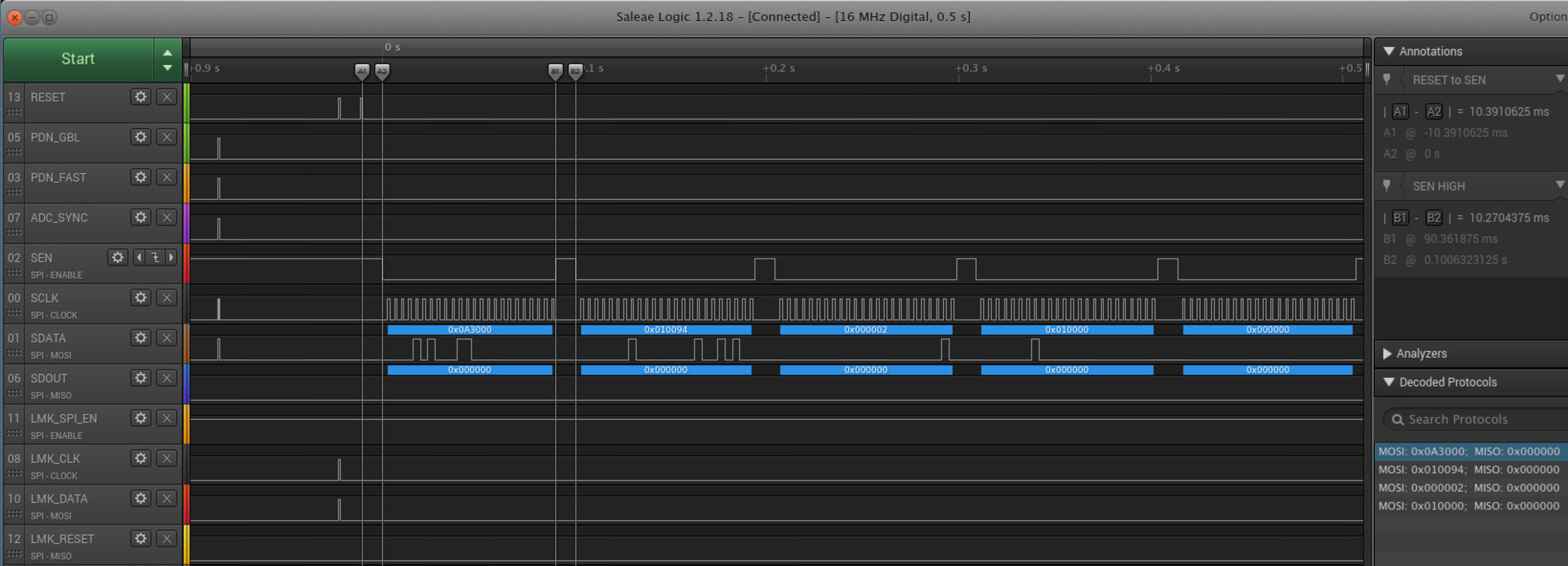
My script sends three SPI transactions to the ADS52J90. I'm probing the signals on the eval board using a Salaea logic analyzer to verify the waveforms to the ADC chip. 

1. Write register 0x0A = 0x33 to initialize the chip.

2. Write register 0x00 = 0x02 to enable readback.


3. Read register 0x00 to verify readback mode.

What am I missing? I cannot figure out why the ADC chip always reads back 0.

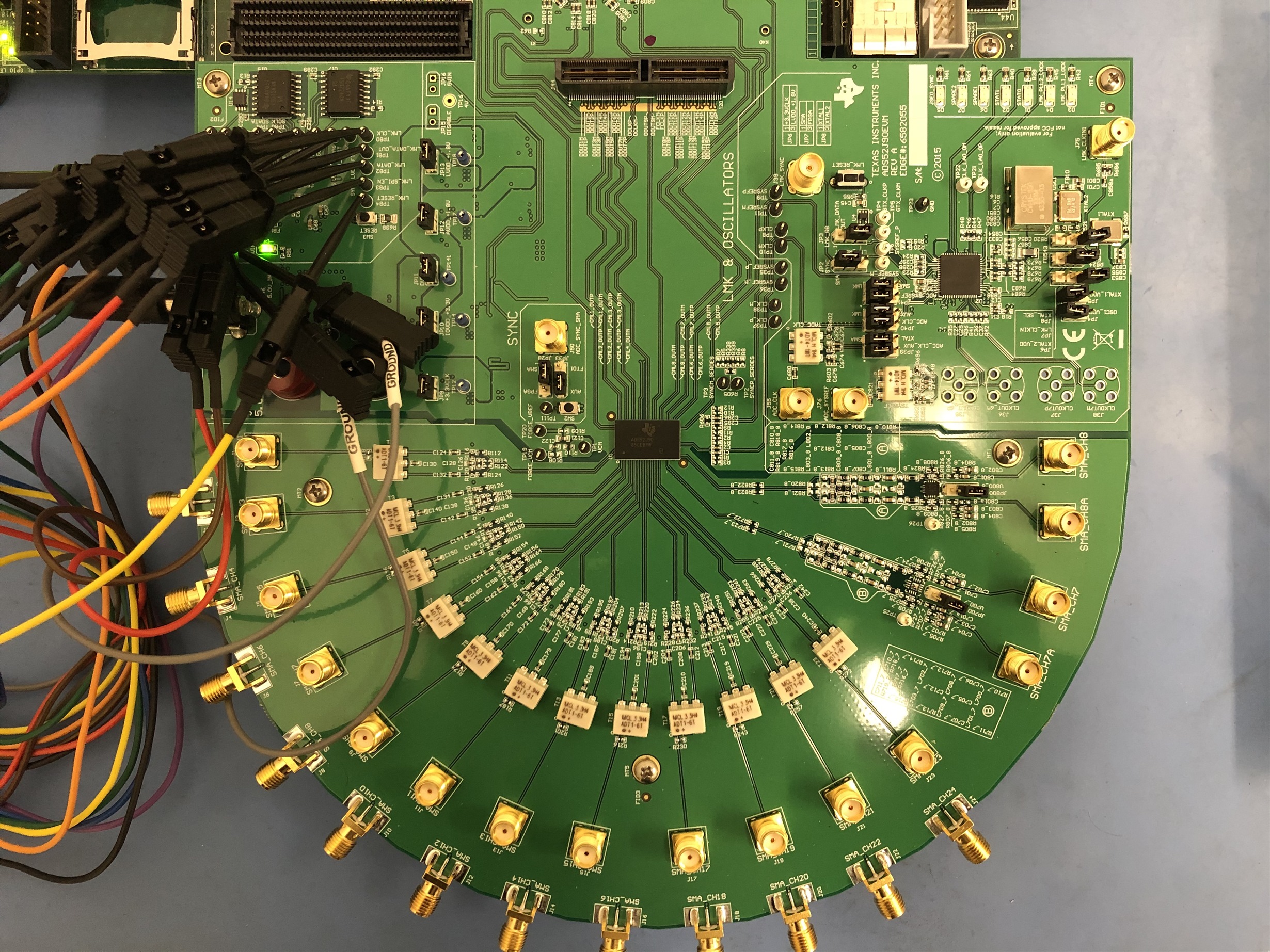
To add to the confusion, I'm working remotely and don't have physical access this hardware board due to the corona virus response. This is the best picture that I have of my probe configuration. I can't quite see all the probe connections for the ADS52J90 adc chip underneath the LMK04826 probes.

Thanks,

Chris

  • Hi,

    Thanks for using ADS52J90EVM.

    we will look into your question and reply to you soon.

    Thank you!

    Best regards,

    Chen

  • Hi,

    How are you?

    According to your concern about the Readback enable register,

    could you at first please setup some other register you want to try (in this case, Readback=Disabled)?

    and after that, then try to set Readback = enable.

    and then please read that register value back (which you just set)

    and then please turn Readback = Disabled

    Hopefully your readback register value is the same as you just set.

    Hopefully it is working fine for you.

    Thank you!

    Best regards,

    Chen

  • I tried setting the ADC into 16-channel input mode and reading back the register, but I still read back all zeros on each SPI read.

    1. Write register 0x0A = 0x0033 to initialize the chip.

    2. Configure 16-channel input mode. Write register 0x01 = 0x0094.

    3. Write register 0x00 = 0x0002 to enable readback.

    4. Read register 0x01 to verify 16-channel input mode. This fails and I only read back zeros.

    5. Read register 0x00 to verify readback mode enabled. This also fails and I see that readback mode is not enabled.

    I'm getting a coworker into my office tomorrow to confirm all the probe connections are correct.

    Thanks,

    Chris

  • Hi,

    Thank you!

    Could you please try the followings?

    1) when SEN turns HIGH, could you please let this HIGH stay longer (for example, >=2 clocks)?

    2) on the test sequence No. 4 shows:

    SDATA's falling edge is too close to SCLK's rising edge.

    Could you please avoid it?

    Hopefully these two can help.

    Thank you!

    Best regards,

    Chen

  • I tried all of this and still have not read anything back other than 0. 

    1. I don't think the SEN high time was an issue because I'm bit-banging this interface with python and it is really slow. The time scale for all my captures is in milliseconds. Is there any issue clocking this interface too slowly? I didn't see any minimum SCLK requirements in the datasheet.

    2. I cleaned up the waveform so that I don't have any falling edges close to the SCLK rising edge. See below.

    3. I noticed on page 90-91 of the ADS52J90 datasheet power sequencing recommendations that the sample clock is shown to be clocking before the SPI register setup. Is the sample clock required to be clocking for the register interface to write and read back properly? I don't think I have setup the LMK04826 clock distribution chip and/or board connections for the sample clock to be running yet. Only the SCLK is running for the SPI transactions.

    4. I can see that the PDN_XXX pins are driven high briefly when the bit-bang interface is initialized. This happens more than 80 milliseconds before the first SPI write. This shouldn't be a problem, correct?

  • Hi,

    Also please also look at the datasheet more details on its page 8

    it mentions: SDOUT is 1.8V logic.

    Please make sure from your setting from your side.

    if not, then your FPGA cannot read its output data at all.

    =========

    SDOUT      C5    Output
    Serial interface data readout. High impedance when readout is disabled. 1.8-V logic level is recommended.

    =========

    Thank you!

  • Hi,

    Could you please let us know?

    1) Do you connect ADS52J90EVM Board's USB connector to your PC's USB connector?

    We recommend at the first try, please do so.

    In this case, you can use ADS52J90 GUI to fully control all the register controls by using ADS52J90's GUI on your PC.

    And you can 100% check how the Readout function works.

    This can help you a lot before you try to move this to your FPGA control.

  • To be clear, I'm connecting my PC USB to the ADS52J90EVM board for this test. I used the Salaea Logic 16 to analyze the SPI transactions. This device supports a 1.8V voltage thresholds. This seems to be working because it is showing all the other 1.8V threshold lines going to the ADC from the FTDI FT4232 chip on the ADS52J90EVM.

    I do not have one of the TI supported host FPGA cards (TSW14J56EVM or TSW1400) expected by the GUI control. I'm connecting the ADS52J90EVM board to a Xilinx ZC706 through the high pin count FMC connector. Is it possible to use the GUI ( HMC-DAQ, High Speed Data Converter Pro, etc) with an ADS52J90EVM and no TI approved host card to configure the ADC registers? I'd be happy to try that, but it seemed like there was no way to program the ADC on the ADS52J90EVM without a card like the TSW14J56EVM plugged in as well.

  • Hi,

    Thank you for your detail description.

    For using ADS52J90EVM then please follow ADS52J90EVM User's Guide,

    that is the only support (described inside) such as TSW1400 and/or TSW14J56 boards.

    but other TSW boards or Xilinx board or FMC connector (which may be supported by other devices) connections are not supported by our ADS52J90 bench test. That is why we try to understand whether you are using TSW1400 or TSW14J56 capture boards or not.

    Since you are using ADS52J90EVM which the SPI is still controlled by using FT4232 chip,

    however we need to double check if we can only use ADS52J90 GUI only (without using TSW1400 or TSW14J56) for controlling registers purpose or not.

    We will try it and let you know later.

    Thank you!

    Best regardfs,

    Chen

  • Hi,

    We hare verified again and found ADS52J90EVM GUI is directly related to High Speed Data Converter Pro (HSDC Pro) GUI.

    Therefore if you don't have TSW1400 or TSW14J56 Board that includes their GUI as well,

    then you cannot run ADS52J90 GUI at all.

    Therefore in that case, you need to set up ADS52J90 register settings by yourself

    that could make it more difficult to let us try to track what you are setting as the same as we are doing

    using our ADS52J90 EVM and its GUI together.

    Just need to confirm this with you.

    Thank you!

    Best regards,

    Chen