This thread has been locked.

If you have a related question, please click the "Ask a related question" button in the top right corner. The newly created question will be automatically linked to this question.

ADS8556: ADS8556 internal reference DAC not responding to changes

Part Number: ADS8556

Hello TI support,

im trying to build up an analog frontend with the ADS8556 chip. The circuit is shown in the appended PDF. The ADS is used in software mode to configure the internal registers and control the reference DAC output voltage. The ADC is controlled via an ESP32 using its SPI. I'm writing the 32 Bit number 11111110 00000001 00000010 11111111 to it with every readout of the measured values. I controlled the SDI line of the ADC via an oscillosciope and the correct bitpattern is send. But the ADC's REFIO pin still remains exactly 2.5V, no matt what DAC pattern I put in. Even changing bit C18 (VREF) to 1, which should result in 3V reference voltage, doesn't change anything.

I would be really happy if there are any ideas why it isn't working.

Tanks!

0247.ADC.pdf

  • Hello,

    From what you are explaining it does seem you are doing it correctly.

    One thing to check is if the Vref is affecting the reading of the conversion even though the voltage change cannot be measured in the REFIO pin

    When at Vref=2.5V, enter a known DC input and record the reading. Then change the CR to Vref to 3V (11111110 00000101 0100000011 11111111)

    Using the same input vale as before, record the measurement with the new reference value. There should be a change in measurement if the reference voltage was changed.

    Your schematic looks good as well.

    Regards

    Cynthia

  • Hallo Cynthia,

    thanks for your reply!

    I testet it with the 3V reference bit before and now again. Like I said there's no change on the REFIO pin. Now I checked the measured values too, but they behave the same. Between CR18 set or not set is no difference in code values.

    Regards

    Michael

  • Michael,

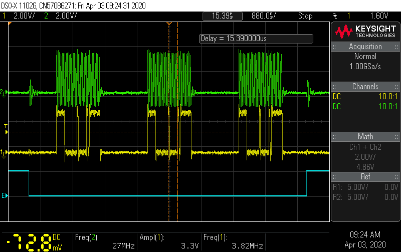
    Thank you for trying that, would you please provide a scope shot of the digital communications line, including FS, SCLK, SDI

    Regards, Cynthia

  • Sure,

    thanks for your help!

    The first image contains a complete cycle of transmission. I read out 3x32 bit of the ADC and write 3 times the control register content to it. Green is CLK, yellow SDI and blue FS.

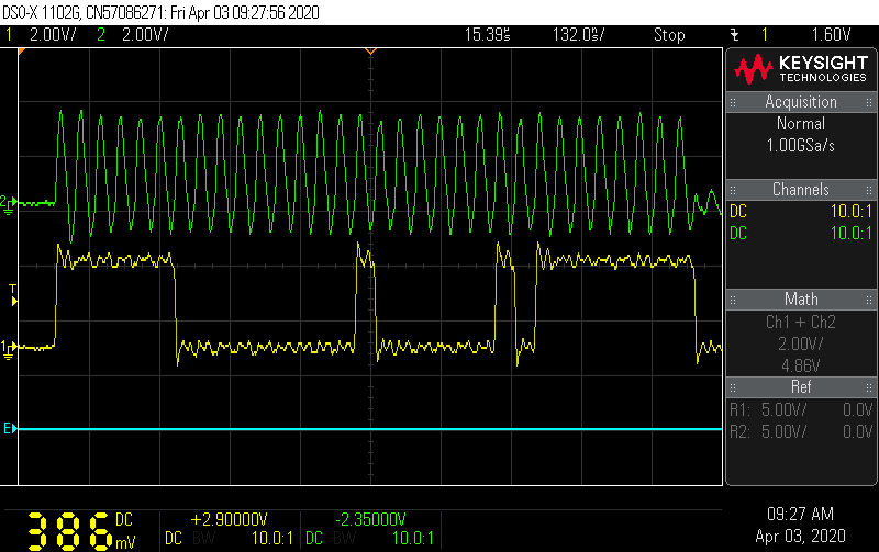
    On the second image is only one 32bit transmission shown, to see better whats happening, the FS is still low.

    (Second image)

    Regards

    Michael

  • Let's check that the deice is initiated correctly. Please check that the STBY pin is at a logic high voltage.

    Once this is verified please try the following. This will update the register content and read it back to confirm that the contents have been updated.

    1. Writing the 32 Bit data 11111110  00000111  00000011  11111111 to ADC  (highlighted in red to show difference)

    2. Send a CONVST high pulse signal to ADC (>1.3us).

    3. Monitor BUSY signal. When it changes from high to low (falling edge of BUSY) read data on SDO with /CS to see if CR register data is shown. Also, check if the voltage on REFIO pin has been changed to 3V.

    Regards

    Cynthia

  • Thanks for your advice!

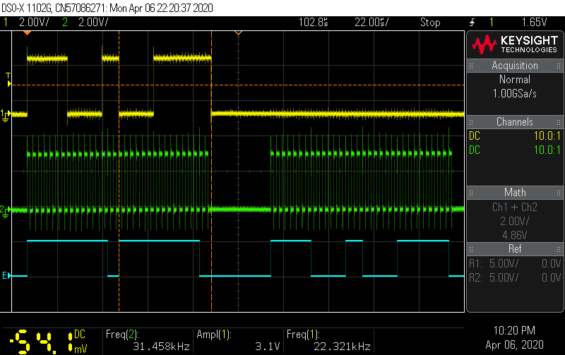
    I'v done it like you told and monitored it with the oscilloscope, shown in the screenshot (channel 1 SDI, channel 2 CLK, channel 3(EX) SDO).

    Interestingly this yields 1.24V on the REFIO pin.

    Regards

    Michael

  • Thanks, this is good information.

    The SDO read out, if I am looking correctly, has the last bit low, although it was programed to be high. So it does seem that there is a discrepancy.

    Would you confirm that you are using SPI mode1? The SDI and SDO data should change state at rising edges of SCLK, and be read on falling edges of SCLK.

    Can we test something else out. After powering up the ADC, send a reset pulse to reset the device. Do not program CR register and just read internal CR register content directly by writing the 32 Bit data to ADC. The REFIO voltage should be 2.5V and should read as so in the CR content. please provide timing plot. Please include CS in the screenshots as well.

    00000010  00000010  00000011  11111111

    Looking at the timing diagram to update the CS, shown below, there are a few aspects that need to be considered.

    Note that the BUSY signal goes high after the first frame, this means that a CONVST was initiated between the two frames. after the first frame, you need to be sure to toggle CONVST and wait until BUSY goes low again before the second frame. Also, be mindful of the state of CS, as this also needs to be low.

    Regards

    Cynthia