This thread has been locked.

If you have a related question, please click the "Ask a related question" button in the top right corner. The newly created question will be automatically linked to this question.

ADS131M08: What's the common mode input range of ADS131M08?

Part Number: ADS131M08
Other Parts Discussed in Thread: ADS131E08, STRIKE

Hi Expert,

I am using ADS131M08 and can you make me clear about below questions?

1. I didn't find the Vcm range of ADS131M08 in datasheet, what is the Vcm range of this device?

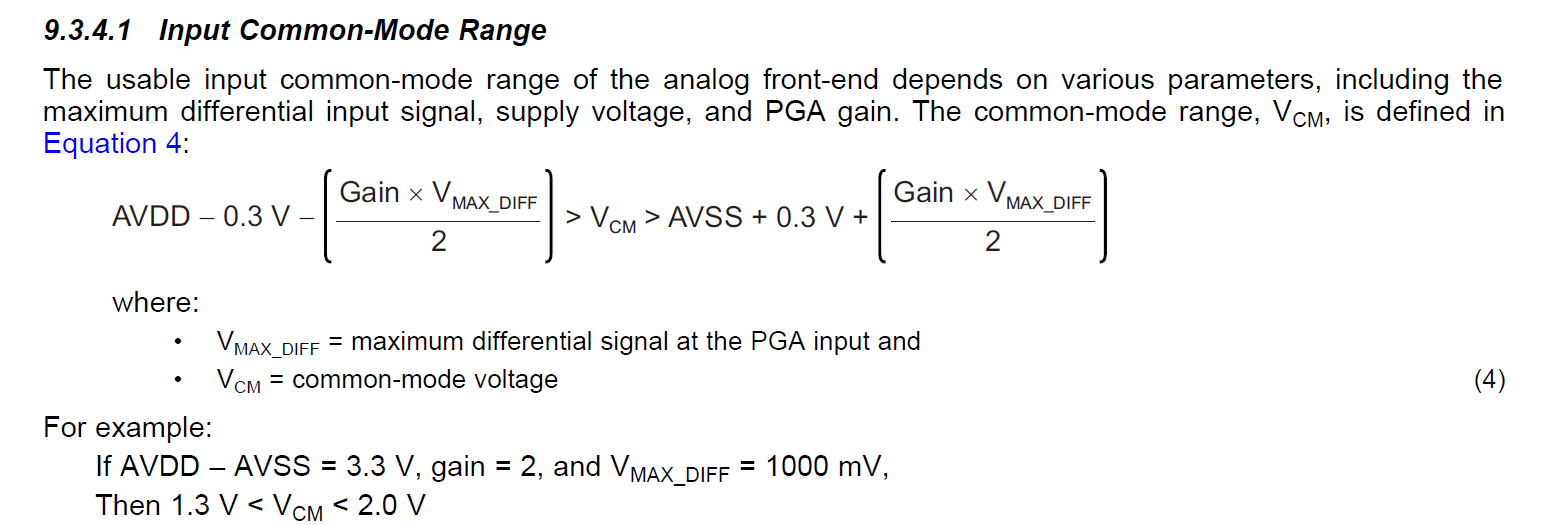
2.I am also considering ADS131E08, and luckily I found a detailed Vcm range description, is ADS131M08 Vcm range same as E08 or not?

3.In my opinion, Vcm = (VINxP + VINxN) / 2, but the definition for Vcm of ADS131E08 is different, see below datasheet description(says Vcm = (VINxP - VINxN) / 2), is it a typo in datasheet?

4.Can I float the GND of ADS131M08 in a differential mode sample input? Is there any potential risk in EMC test if I use floating ADS131M08 GND ?  

Thank you.

Rachel 

  • Rachel,


    Thanks for your questions about the ADS131M08. I'll just answer these questions in order.

    1. The ADS131M08 has an input range that is dependent on the PGA gain that is used. You can see this in the Recommended Operating Conditions table on page 5 of the datasheet.

    For Gain=1, 2, 4, the inputs can be anywhere from AGND-1.3V to AVDD. With higher gains, the precharge buffer limits the top end range from AGND-1.3V to AVDD-1.8V. In both cases, the input can go below GND because of a negative charge pump in the device.

    2. The ADS131E08 has a different input range because of the nature of the PGA. In the ADS131E08, the PGA is implemented with a real amplifier, where it's constructed similar to the front end of an instrumentation amplifier. Because the PGA input and output have the same common-mode voltage, the output is more limited when the PGA gain is high.

    For the ADS131M08, the PGA implementation is different. In both devices, the ADC capacitively samples the input voltage and compares it to a capacitively sampled reference. In the ADS131M08, instead of using an amplifier to add gain to the input signal, the device can change the size of the sampling capacitor. For example, if you want to increase the gain by a factor of 2, you could either double the size of the input sampling capacitance and keep the same reference sampling capacitance. Or you could keep the same input sampling capacitance, and halve the reference sampling capacitance. There's also scaling that can be done in the digital section.

    Regardless, the ADS131M08 and the ADS131E08 do not use the same type of PGA implementation.

    3. You are correct, this appears to be an error in the datasheet. The common-mode voltage is midway between the AINP and AINN signal. To be correct, it should be:

    VCM = (V(INxP)+V(INxN))/2

    4. You should not be floating the GND for the device. For any measurement, the device must have a defined common-mode voltage that is with the given input range. The ground should be well defined. Additionally any potential ESD strike might use the GND to shunt away current through ESD diodes.

    Hopefully, that clears up your questions. If I've missed or misunderstood something, post back and ask again.


    Joseph Wu

  • Hi Joseph,

    Thank you very much.

    I do have one more question to confirm ADS131M08 common-mode input range. Let's take Gain=1, so the VAINxP and VAINxN can range from AGND-1.3 to AVDD,

    so what range can the common-mode input be? Is it (AGND-1.3+AGND-1.3)/2 to (AVDD+AVDD)/2 = AGND-1.3 to AVDD ?

    Thank you!

  • Hi,

    Yes, that is correct. With a gain of 1, the common mode input range is basically AGND-1.3V to AVDD. This is also the limits for the absolute input voltage, so with a that as the common-mode input range, the differential input at that point must basically be 0V.

    Joseph Wu

  • Hi Joseph,

    Thanks a lot.

    I do have another question for GUI. Since different topic, I post another question.

    Thanks!

    R