This thread has been locked.

If you have a related question, please click the "Ask a related question" button in the top right corner. The newly created question will be automatically linked to this question.

ADS7830: how to minimize the error of reading back data in ADS7830

Part Number: ADS7830
Other Parts Discussed in Thread: ADS7828, ADC128D818

Hi Team,

Customer used ADS7830 to monitor the voltage and find the error this lightly large. Could check if the data is right or have a way to optimize?

----------------------------

We verified ADS7830 function on two units - compare the actual voltage measured at ADS7830 pin and the voltage reported by ADS7830

Test results on some channels exceed ADS7830 accuracy spec. See attached file for details. 

Column B - Actual voltage measured at ADS7830 pin

Column D - Voltage reported by ADS7830

Column E - Difference between two voltages above

Our design is as below. 

Could you help to check and advise the reason for the failures?

Sample1 Default Voltage
Channel Actual voltage measured at ADS7830 pin ADS7830 register ADS7830 Report Voltage Voltage Gap Max "-" Spec
(-0.71 LSB)
Max "+" Spec
(1.22 LSB)
Result
0 0.921 5e 0.91796875 -0.00303125 -0.006933594 0.011914063 PASS
1 0.919 5e 0.91796875 -0.00103125 -0.006933594 0.011914063 PASS
2 0.925 5e 0.91796875 -0.00703125 -0.006933594 0.011914063 FAIL
3 1.811 b9 1.806640625 -0.004359375 -0.006933594 0.011914063 PASS
4 1.678 ab 1.669921875 -0.008078125 -0.006933594 0.011914063 FAIL
5 1.622 a6 1.62109375 -0.00090625 -0.006933594 0.011914063 PASS
6 1.568 a0 1.5625 -0.0055 -0.006933594 0.011914063 PASS
7 1.721 b0 1.71875 -0.00225 -0.006933594 0.011914063 PASS
Sample1 High Voltage
Channel Actual voltage measured at ADS7830 pin ADS7830 register ADS7830 Report Voltage Voltage Gap Max "-" Spec
(-0.71 LSB)
Max "+" Spec
(1.22 LSB)
Result
0 0.942 60 0.9375 -0.0045 -0.006933594 0.011914063 PASS
1 0.938 60 0.9375 -0.0005 -0.006933594 0.011914063 PASS
2 0.934 5f 0.927734375 -0.006265625 -0.006933594 0.011914063 PASS
3 1.902 c2 1.89453125 -0.00746875 -0.006933594 0.011914063 FAIL
Sample1 Low Voltage            
Channel Actual voltage measured at ADS7830 pin ADS7830 register ADS7830 Report Voltage Voltage Gap Max "-" Spec
(-0.71 LSB)
Max "+" Spec
(1.22 LSB)
Result
0 0.906 5c 0.8984375 -0.0075625 -0.006933594 0.011914063 FAIL
1 0.896 5b 0.888671875 -0.007328125 -0.006933594 0.011914063 FAIL
2 0.9 5c 0.8984375 -0.0015625 -0.006933594 0.011914063 PASS
3 1.723 b0 1.71875 -0.00425 -0.006933594 0.011914063 PASS
Sample1 Default Voltage
Channel Actual voltage measured at ADS7830 pin ADS7830 register ADS7830 Report Voltage Voltage Gap Max "-" Spec
(-0.71 LSB)
Max "+" Spec
(1.22 LSB)
Result
0 0.922 5e 0.91796875 -0.00403125 -0.006933594 0.011914063 PASS
1 0.921 5e 0.91796875 -0.00303125 -0.006933594 0.011914063 PASS
2 0.923 5e 0.91796875 -0.00503125 -0.006933594 0.011914063 PASS
3 1.806 b8 1.796875 -0.009125 -0.006933594 0.011914063 FAIL
4 1.675 ab 1.669921875 -0.005078125 -0.006933594 0.011914063 PASS
5 1.621 a5 1.611328125 -0.009671875 -0.006933594 0.011914063 FAIL
6 1.568 a0 1.5625 -0.0055 -0.006933594 0.011914063 PASS
7 1.718 af 1.708984375 -0.009015625 -0.006933594 0.011914063 FAIL
Sample1 High Voltage
Channel Actual voltage measured at ADS7830 pin ADS7830 register ADS7830 Report Voltage Voltage Gap Max "-" Spec
(-0.71 LSB)
Max "+" Spec
(1.22 LSB)
Result
0 0.943 60 0.9375 -0.0055 -0.006933594 0.011914063 PASS
1 0.94 60 0.9375 -0.0025 -0.006933594 0.011914063 PASS
2 0.932 5f 0.927734375 -0.004265625 -0.006933594 0.011914063 PASS
3 1.896 c2 1.89453125 -0.00146875 -0.006933594 0.011914063 PASS
Sample1 Low Voltage
Channel Actual voltage measured at ADS7830 pin ADS7830 register ADS7830 Report Voltage Voltage Gap Max "-" Spec
(-0.71 LSB)
Max "+" Spec
(1.22 LSB)
Result
0 0.906 5c 0.8984375 -0.0075625 -0.006933594 0.011914063 FAIL
1 0.898 5c 0.8984375 0.0004375 -0.006933594 0.011914063 PASS
2 0.899 5c 0.8984375 -0.0005625 -0.006933594 0.011914063 PASS
3 1.718 af 1.708984375 -0.009015625 -0.006933594 0.011914063 FAIL

Thanks.

  • Hello,

    Would you please explain how the max and min specs were come to?

    I believe what you are looking for here is the total unadjusted error; there is a great three part blog explaining the topic of ADC accuracy, in particular part 2: total unadjusted Error, that I believe would directly address this issue.

    I also notice that the difference between the pin voltage and ADC output is greater than half an LSB. the ADC should settle to half of an LSB or less. This could also be leading to the greater than expected error.  When using the internal 2.5V, the LSB= 12.89mV, which then means settling goal for the input is half = 6.445V. This would mean that the ADC will output a value reflecting the input, and not be codes off.

    What sampling rate is the devices running at? A quick check to see if it is a settling issue, is slowing down the sampling rate, if the measurements become closer to the expected voltage then it is a settling issue. If so, I would suggest lowering the sampling rate if possible, if not, then we can work together to change the RC filter values to allow for proper settling

    Regards

    Cynthia

  • Hi Cynthia,

    Please refer to my comments and further questions below. Thanks.

    1) Would you please explain how the max and min specs were come to?

    The specs were calculated based on the equation in the link you shared. 

    A recommended way of calculating the maximum TUE at a particular analog input voltage is to take the root-sum-square (RSS) of the maximum values of all individual errors at that point ,(Equation 1). 

    The root-sum-square result is -0.71 LSB ~ +1.225 LSB. 

    Would you please advise if any concerns on this result?


    2) When using the internal 2.5V, the LSB= 12.89mV, which then means settling goal for the input is half = 6.445V. 

    According to previous discussions with TI FAE, the LSB of ADS7830 is 2.5V/256 = 9.7656mV. Would you please advise how the 12.89mV LSB is calculated?


    3) What sampling rate is the devices running at?

    The I2C frequency connecting to ADS7830 is 400k. The host will polling the voltage from ADS7830 every 5s.

    Suppose you are suggesting to change the I2C frequency from 400k to 100k, not enlarging the 5s polling period. Would you please confirm this?

  • Hi Cynthia,

    Please refer to my comments and further questions below. Thanks.

    1) Would you please explain how the max and min specs were come to?

    The max and min specs were calculated based on the equation in the link you shared. part 2: total unadjusted Error

    A recommended way of calculating the maximum TUE at a particular analog input voltage is to take the root-sum-square (RSS) of the maximum values of all individual errors at that point ,(Equation 1). 

    The root-sum-square result is -0.71 LSB ~ +1.22 LSB.

    Would you please advise if any concerns on this result?

    2) When using the internal 2.5V, the LSB= 12.89mV, which then means settling goal for the input is half = 6.445V.

    According to previous discussions with TI FAE, the LSB is 2.5V/256 = 9.7656mV. Would you please advise how 12.89mV is calculated?

    3) What sampling rate is the devices running at? 

    The I2C frequency connecting to ADS7830 is 400k. The host polling ADS7830 voltage result every 5s. 

    Suppose you are suggesting to change I2C frequency from 400k to 100k, not enlarging the 5s polling period. 

    Would you please help to confirm this?

  • 1. Can you share exactly what numbers are used here?  I am not getting the same numbers.

    I am using  the following and get slightly different results of  +/-0.52LSB and +/-1.32LSB.

    On top of this, please also note that the internal voltage reference has a max and min of 2.48V to 2.52V that is 20mV in either direction. the TUE does not consider the reference not calibration. the customer can measure the actual voltage at the REF pin, and use that value to interpret the ADC measurements.

    Squared
    Spec Min Max Min Max
    INL -0.1 0.5 0.01 0.25
    DNL -0.1 0.5 0.01 0.25
    offset 0.5 1 0.25 1
    Gain -0.1 0.5 0.01 0.25
    Sum 0.28 1.75
    TUE 0.52915 1.3228757

    2. You are correct, I was using the wrong resolution size. for 8 bits, and full scale of 2.5V. the LSB is = 2.5/2^8 = 2.5/256 = 9.765mV

    3. I would suggest looking at question 1 first, before trying the below.

    You do not need to change the clock rate, thus the throughout will remain the same. What will need to change is the time between the command byte to the device and the next read address byte. When the device receives a command byte, the acquisition mode begins when BIT 4 is received, this is when the input is being sampled, elongating this time will allow for longer settling time. the acquisition time ends with the next read addressing command.

    Regards

    Cynthia

  • Hi Cynthia,

    I will check on your suggestions. Would you please help to double confirm this question firstly?

    For the resolution size, there is a note (1) in ADS7830 datasheet:

    It shows when Vref=2.5V, 1LSB is 9.8mV. (2.5V/9.8mV=255). 

    After changing the resolution size from 9.765mV(2.5V/256) from 9.8mV(2.5V/255) for calculation, the calculated result is more close to the measurement result. 

    I am wondering if ADS7830 has some specific design internally to match 2.5V/255 resolution zise, other than 2.5V/256. 

    Would you please double confirm this? 2.5V/255 or 2.5V/256 is the correct calculation approach of resolution size for ADS7830?

    Thanks.

  • Hi Cynthia,

    Apart from the resolution size definition, I have one more question about the TUE calculation. I combine two questions into this mail. Would you please advise? Thanks.

    1) For the resolution size, there is a note (1) in ADS7830 datasheet:

    It shows when Vref=2.5V, 1LSB is 9.8mV. (2.5V/9.8mV=255). 

    After changing the resolution size from 9.765mV(2.5V/256) from 9.8mV(2.5V/255) for calculation, the calculated result is more close to the measurement result. 

    I am wondering if ADS7830 has some specific design internally to match 2.5V/255 resolution zise, other than 2.5V/256. 

    Would you please double confirm this? 2.5V/255 or 2.5V/256 is the correct calculation approach of resolution size for ADS7830?

    2) For TUE calculation, let's focus on the Max TUE case firstly, which is our main concern currently. 

    In your TUE calculation, all the 4 types of errors (INL, DNL, Offset, Gain) are accounted in. 

    To my understanding, the INL error has already covered the DNL error. Then the DNL should be ruled out from TUE calculation. In other words, only 3 types of errors (INL, Offset, Gain) should be accounted for TUE calculation. 

    In the link part 2: total unadjusted Error you shared, it also only contains 3 types of errors (INL, Offset, Gain; no DNL) in TUE calculation equation. 

    That's the way I got the Max TUE 1.22 LSB. 

    Would you please double check if anything wrong with my understanding? 

  • Hello,

    To address the resolution question, it is not a matter of codes, 255 vs 256. It has to do more with rounding.

    2.5/255 = 9.8mV

    2.5/256 =9.765mV

    The device probably cannot reach into the microvolt level, thus rounded to 9.8mV


    The blog was trying to simply in effort to keep the write up short, thus only used three of the four, but the INL and the DNL should both be included. In equation 1, there are "…" to indicate there are more, the equation is just shortened for simplicity. but all four DC specifications should be used. 

    In the document, Glossary for ADC Specifications, the Total unadjusted error shows all DC specifications, offset, gain, INL and DNL.


    Regards, Cynthia

  • Hi Cynthia,

    1) For the resolution size, understood that it is not matter of codes.

    To simply my question, for ADS7830, does the exact LSB equal to 9.8mv (according to datasheet) or 9.765mv (calculated by 2.5V/256)?

    As confirmed by TI FAE before, using 9.765mv as 1 LSB is more precise. We also agreed that 2.5V/256 is the common definition of 1 LSB.

    However, our measurement results on these 2 samples show there is less deviation (between actual measured voltage and ADS7830 reported voltage) if using 9.8mv other than 9.765mv as 1LSB. (I will measure several more samples to double confirm the trend).

    Meanwhile, would you please help to double confirm, theoretically, should we use 9.8mv or 9.765mv as 1LSB for ADS7830? Which one is more precise? 

    2) It is noticed that the Max positive and negative tolerance spec is different for ADS7830. 

    Max Positive Max Negative
    INL 0.5 0.5
    DNL 0.5 0.5
    Offset 1
    Gain 0.5 0.5

    Would you please help to confirm the definition of positive and negative tolerance? 

    For "+ positive tolerance" means:

    voltage reported by IC > actual voltage
    or
    actual value > voltage reported by IC

    3) As to the TUE calculation, I still have concerns about the INL and DNL. 

    DNL is the difference between an ideal code width and the measured code width. 

    INL is the deviation between an actual code transition point and its corresponding ideal transition point.

    In my mind, the INL has already included the DNL impact at that point and the total sum of DNL impact at previous points. Then no need to sum DNL in addition to INL again. 

    Would you please advise if anything wrong with my understanding?

  • 1. I agree with you that it is more precise to use the 9.765mV as LSB, but if the device cannot support that level of accuracy, then it is not sustainable to use that value. I had not seen the note previously, until you pointed it out. I am working to get some insight into this from the design team, but I predict that the LSB value to be used is 9.8mV as stated in the datasheet.

    2. It would be: voltage reported by IC > actual voltage

    3. The DNL is needed to measure the INL, perhaps this is the confusion. Also, in delta sigma ADCs, the DNL is not used because of the nature of the device. But in SAR ADCs, they are still two different measurements, and each should be considered.

    Regards

    Cynthia

  • Hi Cynthia,

    Please find my comments below.

    1. I agree with you that it is more precise to use the 9.765mV as LSB, but if the device cannot support that level of accuracy, then it is not sustainable to use that value. I had not seen the note previously, until you pointed it out. I am working to get some insight into this from the design team, but I predict that the LSB value to be used is 9.8mV as stated in the datasheet.

    Appreciated

    Some updates from my side. I measured 4 more units, but the test results varies. On 2 units, the test result align with the 2 first two samples, the voltage calculated based on 9.8mv is more close to the actual voltage than 9.765mv. However, on the other 2 units, the result is reversed - the voltage calculated based on 9.765mv is more close to actual voltage. 

    It is very important to clarify the LSB definition firstly, then we can focus on the correct unit for further debug. 

    2. It would be: (positive error means) voltage reported by IC > actual voltage

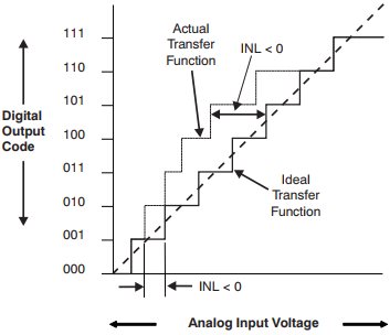
    I revisited the document you shared Glossary for ADC Specifications and find the following figure. 

    It shows the when INL<0 (my understanding is negative error), the voltage reported by IC (actual transfer function) > actual voltage (Ideal transfer function). 

    Would you please double check if anything wrong with my understanding?

    3. For the sampling rate suggestions, I get the following feedback internally.

    Our software cannot control the the time between the command byte to the device and the next read address byte. This interval is controlled by the host IC firmware (IC firmware integrated I2C driver), which is not accessible for our software.

    Our software can control the interval between the current command byte to the next command byte. We are wondering whether it also helps if enlarge the interval between two command bytes. Would you please advise on this?

  • 1. Will get back to you

    2. There is a table to the right of that explaining negative and positive INL error.

    Let's take the example shown in the diagram. the error shows an output of 101. Ideally, say this output corresponds to 1.5 volt.

    BUT the device transitioned earlier (dashed) than the ideal (solid) line, meaning the voltage that made it transition was lower than the ideal 1.5V. In other words, the actual voltage at the input was 1.25V, but the measured output was 1.5V, and this is negative INL.

    For positive INL, the device transitions  after the ideal. using the same example, the input would be at 1.75V but the device would measure out 1.5V

    3. Unfortunately that will not elongate the sampling mode.

    Regards

    Cynthia

  • Hi Cynthia,

    I summarize several points based on our discussions these days. 

    1) TUE calculation should follow the equation below - INL, DNL, OFFSET, GAIN errors should be accounted in for RSS calculation. 

    For ADS7830,

    2) Positive error means ADS7830 reported voltage < actual voltage

    Negative error means ADS7830 reported voltage > actual voltage

    For ADS7830, the reported voltage deviation should be within - 1.33 LSB ~ + 0.85 LSB ("actual voltage - 1.33 LSB" ~ "actual voltage + 0.85 LSB"). 

    3) LSB definition is under confirmation. 

    For the next step of this issue debug, would you please advise the following two more questions?

    1) For sampling mode change, does it help if we slow down the I2C frequency from 400K to 100K?

    2) Apart from the sampling mode change, any other debug suggestions? 


    Thanks.

  • Hi Cynthia,

    Any updates on the 1LSB value definition?

    Additionally, would you please advise the next steps for this issue debug? 

    Thanks.

  • Hello Eric,

    Yes, it seems that the datasheet was estimating, but the device does indeed use the real value of 9.765mV as the LSB.

    using all for of the DC errors, the max TUE would be, 1.322 LSB, and min of 0.529 LSB

    if you are still getting readings further than this, I would look at possible sources of error such as the analog power supply and the input drive.

    You had mentioned that the input can be seen across all channels, at different input scenarios. I find it interesting that Ch6 has not failed, this is correct?

    If so, that is a good indicator of how small the resistors can be while paired with the 0.1uF cap. Decreasing the capacitor allows for larger caps.

    On the input channels without the voltage divider, I would suggest decreasing the resistor size to 1K, if keeping the capacitor. If decreasing the cap, the resistor can be a bit larger than the 1k suggested.

    I would suggest decreasing the resistors on the resistor on the voltage dividers as well.

    Regards

    Cynthia

  • Hi Cynthia,

    Thanks for the update. 

    I revisited the previous test results of the 6 units based on 9.765mv LSB definition, -1.322 LSB ~ 0.866 LSB voltage deviation spec. 

    All channels are PASS on 4 units, but 2 units still fails. 

    For failed unit 1, CH3,CH5,CH6,CH7 are over spec. 

    For failed unit 2, CH3, CH6 are over spec. 

    See the table below for the measurement results. 

    Sample1   Normal High Voltage Low Voltage
    Sensor CH Power Rail Register IC Read Measurement δ Max Negative Spec Max Positive Spec Result Register IC Read Measurement δ Max Negative Spec Max Positive Spec Result Register IC Read Measurement δ Max Negative Spec Max Positive Spec Result
    CH0 AVC_PCIE_TX 5e 0.91796875 0.92143 -0.00346125 -0.012919922 0.008457031 PASS 60 0.9375 0.94217 -0.00467 -0.012919922 0.008457031 PASS 5c 0.898438 0.90555 -0.00711 -0.012919922 0.008457031 PASS
    CH1 VDD_0V9 5d 0.90820313 0.91933 -0.011126875 -0.012919922 0.008457031 PASS 5f 0.927734 0.93755 -0.00982 -0.012919922 0.008457031 PASS 5b 0.888672 0.89593 -0.00726 -0.012919922 0.008457031 PASS
    CH2 AVC_PCIE 5e 0.91796875 0.92174 -0.00377125 -0.012919922 0.008457031 PASS 5e 0.917969 0.93074 -0.01277 -0.012919922 0.008457031 PASS 5b 0.888672 0.89719 -0.00852 -0.012919922 0.008457031 PASS
    CH3 VCC_1V8 b8 1.796875 1.8083 -0.011425 -0.012919922 0.008457031 PASS c1 1.884766 1.898 -0.01323 -0.012919922 0.008457031 FAIL af 1.708984 1.719 -0.01002 -0.012919922 0.008457031 PASS
    CH4 VCC_3V3 aa 1.66015625 1.6727 -0.01254375 -0.012919922 0.008457031 PASS N/A N/A N/A N/A N/A N/A N/A N/A N/A N/A N/A N/A N/A N/A
    CH5 VCC_5V a5 1.61132813 1.626 -0.014671875 -0.012919922 0.008457031 FAIL N/A N/A N/A N/A N/A N/A N/A N/A N/A N/A N/A N/A N/A N/A
    CH6 VCC_12V 9f 1.55273438 1.5693 -0.016565625 -0.012919922 0.008457031 FAIL N/A N/A N/A N/A N/A N/A N/A N/A N/A N/A N/A N/A N/A N/A
    CH7 VCC_3V3_AUX af 1.70898438 1.7259 -0.016915625 -0.012919922 0.008457031 FAIL N/A N/A N/A N/A N/A N/A N/A N/A N/A N/A N/A N/A N/A N/A
    Sample2   Normal High Voltage Low Voltage
    Sensor CH Power Rail Register IC Read Measurement δ Max Negative Spec Max Positive Spec Result Register IC Read Measurement δ Max Negative Spec Max Positive Spec Result Register IC Read Measurement δ Max Negative Spec Max Positive Spec Result
    CH0 AVC_PCIE_TX 5e 0.91796875 0.92161 -0.00364125 -0.012919922 0.008457031 PASS 60 0.9375 0.94219 -0.00469 -0.012919922 0.008457031 PASS 5c 0.898438 0.90594 -0.0075 -0.012919922 0.008457031 PASS
    CH1 VDD_0V9 5d 0.90820313 0.91878 -0.010576875 -0.012919922 0.008457031 PASS 5f 0.927734 0.93705 -0.00932 -0.012919922 0.008457031 PASS 5b 0.888672 0.89531 -0.00664 -0.012919922 0.008457031 PASS
    CH2 AVC_PCIE 5e 0.91796875 0.9217 -0.00373125 -0.012919922 0.008457031 PASS 5f 0.927734 0.93086 -0.00313 -0.012919922 0.008457031 PASS 5b 0.888672 0.89711 -0.00844 -0.012919922 0.008457031 PASS
    CH3 VCC_1V8 b8 1.796875 1.811 -0.014125 -0.012919922 0.008457031 FAIL c2 1.894531 1.901 -0.00647 -0.012919922 0.008457031 PASS af 1.708984 1.7219 -0.01292 -0.012919922 0.008457031 PASS
    CH4 VCC_3V3 aa 1.66015625 1.6714 -0.01124375 -0.012919922 0.008457031 PASS N/A N/A N/A N/A N/A N/A N/A N/A N/A N/A N/A N/A N/A N/A
    CH5 VCC_5V a5 1.61132813 1.6198 -0.008471875 -0.012919922 0.008457031 PASS N/A N/A N/A N/A N/A N/A N/A N/A N/A N/A N/A N/A N/A N/A
    CH6 VCC_12V 9f 1.55273438 1.5681 -0.015365625 -0.012919922 0.008457031 FAIL N/A N/A N/A N/A N/A N/A N/A N/A N/A N/A N/A N/A N/A N/A
    CH7 Not Used N/A N/A N/A N/A N/A N/A N/A N/A N/A N/A N/A N/A N/A N/A N/A N/A N/A N/A N/A N/A N/A

    1) I tried to debug on CH3 by changing the in-series resistor from 10k to 1k, but there is no improvement on the voltage deviation. 

    2) I would like to try some more resistance/capacitance for further debug as your suggestions. Would you please advise the recommended resistance and capacitance for ADS7830 application? Or a resistance/capacitance range based on TI's best practice, then I can try it. 

    Thanks.

  • Knowing this knew information, I would first look at the tolerance of the analog supply. Any deviation or noise in the analog supply will directly be seen in the output measurements, as this is used as the reference.

    Then, I would suggest looking first at the tolerance of the resistors being used. Especially with the voltage divider inputs, as each of the resistors will add error. I see in the schematic you provided that you are using 0.1% which can be good enough. But to be sure confirm the tolerance and make sure the measurements will still be good enough with worst error.

    Also, are the inputs in any way oscillating? it seems most are power supplies, thus need to make sure that the inputs are not the cause.

    Are these measurements being done on a solid PCB or through wires connecting multiple connections. if using wires, this can also introduce errors.

    Regards

    Cynthia

  • Hi Cynthia,

    Thanks for your suggestions. As you pointed out, there is deviation of ADS7830 internal reference 2.5V voltage, in a range 2.48V~2.52V. 

    I measured the reference voltage at ADS7830 pin10 on the 2 failed units. Both are not exact 2.5V - one is 2.5154V and the other is 2.5102V. This should be the cause of the voltage deviation issue.

    Use one failed case for example:

    For failed unit CH6, the register is 9F(Hex), while the measurement voltage is 1.5693V.

    In our software, 1 LSB is defined to be 2.5V/256 = 9.765mv, then the reported voltage is 9F(Hex) x 9.765mv = 1.553V. The voltage deviation is 1.5693V-1.553V = 16.3mv > TUE spec

    If calculated with 2.5154V reference voltage, 1 LSB = 2.5154V/256 = 9.826mv. Then the reported voltage is 9F(Hex) x 9.826mv = 1.562V. The voltage deviation is 1.5693V-1.562V = 7.3mv < TUE spec


    Would you please advise if my understanding is correct?

    If yes, here comes the two new questions:

    1) How could our software get the actual internal reference voltage value for calculation? Is there a register to report the actual internal reference voltage value? 

    2) How to minimize the internal reference voltage deviation from 2.5V? Considering the worst case, the internal reference voltage is as worst as 2.52V. There will be 20mv deviation, which is even higher than the TUE spec!

    Thanks.

  • Your understanding is correct, I am glad the source was found.

    There Is no internal register with the reference value unfortunately.

    One method is to use an external reference to provide the voltage, and use a reference that meets the need of the systems

    Another method is measuring the reference with one of the inputs of the device, such as ratiometric measurement, that way any deviation in the reference voltage can be followed.  

    Regards

    Cynthia

  • Hi Cynthia,

    Thanks for your confirmation.

    If calculating with the actual reference voltage value, the original failed items with voltage deviation over TUE now get passed. 

    The following up questions:

    1) About how to minimize the internal reference voltage deviation to 2.5V. 

    Would you please help to double confirm if the actual internal reference voltage is completely controlled by ADS7830 internal circuits - there is no external circuits adjustment would help to reduce its deviation to 2.5V.

    In other words, the current peripheral circuits looks good and no need to fine-tune them further more. 

    2) Got it for your suggestions about using external reference voltage and ratiometric measurement.

    Apart from these two approaches relying on external circuits optimization, would you please advise if TI has any other voltage sense IC products with more precise internal reference voltage? 

    Thanks.

  • 1. I am looking into with design team.

    I would suggest looking at the input circuitry to not be as greatly affected from the Vref variance

    2. The ADS7830 is an 8 bit device, which is likely why there is such variance in the reference. higher resolution devices will have a reference with up to par performance to support it. I did a quick parametric search based on what I know from your system to find some preliminary options.

    I filtered I2C, internal reference, and max resolution to 20 bits. there are 16 results, but these include single channel and multi channel devices

    Results in internal reference with I2C

    Regards

    Cynthia

  • Hi Cynthia,

    For item 1, appreciated if you would get back with some suggestions soon.

    For item 2, I checked the link you shared. There are 2 8-channel ADC with higher resolution (12 bit), ADS7828 and ADC128D818. 

    ADS7828 internal reference voltage deviation spec is even a bit worse than ADS7830. It's 2.475V to 2.525V.

    As for ADC128D818, I did not find its internal reference voltage deviation spec. Would you please help to advise?

    Thanks.

  • 1. The ref capacitor can be increased to help with thermal drift, suggest using a 1uF capacitor. Note that this will only be helpful with temperature drift, and also if a capacitor that also has good drift performance.

    2. The extremes can be estimated using a gaussian distribution, and placing the limits at 3 x standard deviation. the typical is usually one standard deviation

    It would be best to design the input and input drive to introduce the least error as to not be impacted by the reference.

    Regards

    Cynthia

  • Hi Cynthia,

    I am a little confused for this statement. Would you please help to explain more details?

    It would be best to design the input and input drive to introduce the least error as to not be impacted by the reference.


    Not sure if your suggestion is to optimize the circuits of ADS7830 input channels (CH0-CH7), in order to reduce the impact caused by ADS7830 internal reference voltage deviation.

    To my understanding, the input circuits optimization only helps to reduce the unadjusted error, to make ADS7830 calculation result close to the minimal TUE spec, 0.529 LSB.

    However, the additional error caused by ADS7830 internal reference voltage deviation (compared to 2.5V) is independent to the unadjusted error and cannot be reduced.

    In other words, the input circuits optimization only helps to reduce the errors marked in blue color, but has no benefits to the errors marked in red color. (see table below) 

    Please kindly correct me if I did not get your point correctly. Thanks.

    CH Power Rail Typical voltage at ADS7830 input Tolerance when internal reference voltage is 2.48V Max Negative TUE Total Max Negetive tolerance
    (internal reference tolerance+TUE)
    Tolerance when internal reference voltage is 2.52V Max Positive TUE Total Max Positive tolerance
    (internal reference tolerance+TUE)
    0 AVC_PCIE_TX 0.92 -0.00736 -0.012816563 -0.020176563 0.00736 0.008524688 0.015884688
    1 VDD_0V9 0.92 -0.00736 -0.012816563 -0.020176563 0.00736 0.008524688 0.015884688
    2 AVC_PCIE 0.92 -0.00736 -0.012816563 -0.020176563 0.00736 0.008524688 0.015884688
    3 VCC_1V8 1.8 -0.0144 -0.012816563 -0.027216563 0.0144 0.008524688 0.022924688
    4 VCC_3V3 1.65 -0.0132 -0.012816563 -0.026016563 0.0132 0.008524688 0.021724688
    5 VCC_5V 1.598639456 -0.012789116 -0.012816563 -0.025605678 0.012789116 0.008524688 0.021313803
    6 VCC_12V 1.565217391 -0.012521739 -0.012816563 -0.025338302 0.012521739 0.008524688 0.021046427
    7 VCC_3V3_AUX 1.65 -0.0132 -0.012816563 -0.026016563 0.0132 0.008524688 0.021724688
  • Hi Cynthia,

    Any comments on the questions in my last mail? Thanks.

  • Your understanding is correct.

    I was trying to say is to limit dependency of the reference voltage for the input to be within TUE limits.

    Regards

    Cynthia