This thread has been locked.

If you have a related question, please click the "Ask a related question" button in the top right corner. The newly created question will be automatically linked to this question.

ADS131A04: AD conversion value is not returned at multiple device configuration using synchronous slave mode

Part Number: ADS131A04
Other Parts Discussed in Thread: TIDA-00810, CDCLVC1102

AD conversion value is not returned at multiple device configuration using synchronous slave mode.

I conect two ADCs and mode settings are 32bit, no hamming, slave mode.  Also i use 16MHz crystal and set data rate at 16MHz/2/2/512=7812Hz. So i ask AD values every 7812Hz period, but i can't get AD value. AD values are zeros.

How can i get AD values?

  • Kenji-san,


    There are a couple of things that may have happened that prevent you from collecting data.

    First, I would make sure that the device is properly initialized. If you look at Figure 106 on page 79 of the datasheet, there is a flow diagram that shows a startup sequence of the device. Read through it and make sure that your startup sequence matches or is very similar.

    In particular, there are two important commands in the sequence that might be preventing the read. First when the device is first started, an UNLOCK command must be sent to just talk to the device. Second, after the device are confirmed to be ready, you must ENABLE the ADCs with the ADC_ENA register.

    Hopefully, one of these commands will help you get your system working. If you continue to have problems, post back your command sequence, along with the command responses. The ADS131A04 command responses can help you confirm that the device is receiving and properly processing commands.


    Joseph Wu

  • Joseph  Wu-san

    Hi.

    I can't read out the ADC data yet.

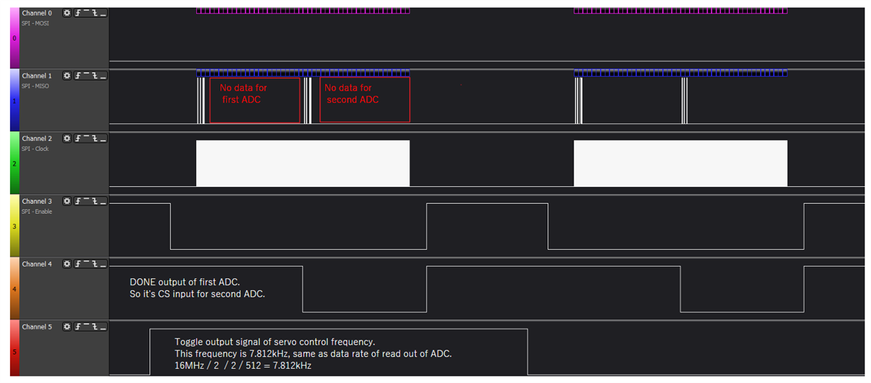
    The logic signal looks like this.

    I initialize the ADC according to the the "initialize set up" flow fig106.

    The control code is based on TI's TIDA-00810LIB.

    Initialization is like this. I omit the verify part of the command.

    ADS131_HardwareInit();

    ADS131_HardwareReset();

    ADS131_Unlock();

    ADS131_SendCommand(WRITE_REGISTER_COMMAND(CLK1, CLK_DIV_2));

    ADS131_SendCommand(WRITE_REGISTER_COMMAND(CLK2, ICLK_DIV_2 | OSR_512));

    ADS131_SendCommand(WRITE_REGISTER_COMMAND(A_SYS_CFG, HRM | A_SYS_CFG_RESERVED));

    // Fixed frame size from now ON

    ADS131_SendCommand_6words(WRITE_REGISTER_COMMAND(D_SYS_CFG, HIZDLY_12ns | DNDLY_12ns | FIXED));

    ADS131_SendCommand_6words(WRITE_REGISTER_COMMAND(ADC_ENA, ADC_ENABLE_ALL_CHANNELS));

    ADS131_Wakeup();

    ADS131_Lock();

    This is the result of reading the register value.

    【Afeter UNLOCK】

    OP_CODE: 2000; address: 0; data: 4
    OP_CODE: 2000; address: 1; data: 3
    OP_CODE: 2000; address: 2; data: 4
    OP_CODE: 2000; address: 3; data: 0
    OP_CODE: 2000; address: 4; data: 0
    OP_CODE: 2000; address: 5; data: 0
    OP_CODE: 2000; address: 6; data: 0
    OP_CODE: 2000; address: 7; data: 6
    OP_CODE: 2000; address: 8; data: 0
    OP_CODE: 2000; address: 9; data: 0
    OP_CODE: 2000; address: a; data: 0
    OP_CODE: 2000; address: b; data: 60
    OP_CODE: 2000; address: c; data: 3c
    OP_CODE: 2000; address: d; data: 8
    OP_CODE: 2000; address: e; data: 86
    OP_CODE: 2000; address: f; data: 0
    OP_CODE: 2000; address: 10; data: 0
    OP_CODE: 2000; address: 11; data: 0
    OP_CODE: 2000; address: 12; data: 0
    OP_CODE: 2000; address: 13; data: 0
    OP_CODE: 2000; address: 14; data: 0

    【Afeter Set Registers】

    OP_CODE: 2000; address: 0; data: 4
    OP_CODE: 2000; address: 1; data: 3
    OP_CODE: 2000; address: 2; data: 14
    OP_CODE: 2000; address: 3; data: c
    OP_CODE: 2000; address: 4; data: c
    OP_CODE: 2000; address: 5; data: 0
    OP_CODE: 2000; address: 6; data: 0
    OP_CODE: 2000; address: 7; data: 6
    OP_CODE: 2000; address: 8; data: 0
    OP_CODE: 2000; address: 9; data: 0
    OP_CODE: 2000; address: a; data: 0
    OP_CODE: 2000; address: b; data: 60
    OP_CODE: 2000; address: c; data: 3e
    OP_CODE: 2000; address: d; data: 2
    OP_CODE: 2000; address: e; data: 25
    OP_CODE: 2000; address: f; data: f
    OP_CODE: 2000; address: 10; data: 0
    OP_CODE: 2000; address: 11; data: 0
    OP_CODE: 2000; address: 12; data: 0
    OP_CODE: 2000; address: 13; data: 0
    OP_CODE: 2000; address: 14; data: 0

    Checking the command response, it seems that the initialization is ok.
    After initialize, i ask ADC data every 7.812 KHz, at servo control frequency.

    STAT_1, bit flag F_RESYNC is "1" when read out ADC data. So resynchronization is fault.
    How do I communicate between ADC and MCU to read out data every 7.812kHz?
    I refer to Figure 96 and Figure 66, but I don't know the right way.
    I think there is information that is not described in the specifications regarding the timing of communication.

  • Kenji-san,

    Looking through the initialization sequence, it looks ok. This is very similar (if not the same as the one shown in Figure 106 on page 79 of the datasheet. I would note that the setup described in TIDA-00810 uses one device in asynchronous interrupt mode and a daisy chained device in synchronous slave mode. This is also similar to the connection shown in Figure 96 on page 69 the datasheet with the Multiple Device Configuration Using Asynchronous Interrupt Mode. Can you share your schematic? I want to confirm that you have the devices connected this way so that the daisy chain operates properly.

    For the communication, it's important to see the command responses too. At this point, it's likely that the device doesn't understand one of the commands or has some miscommunication. The command responses can help easily debug which command is not being understood by the device. With the screen shots of the digital communication, I can see that you are using a Saleae. If you want, you can attach the data file to the next post, so I can read through the SPI response too (I have a Saleae with the software also).

    I would note that the synchronization must be exact. The timing for the ADS131A04 is strict in synchronous slave mode, and the the timing should be 7.8125kHz. If you use the first device in asynchronous interrupt mode, then the /DRDY line acts as the synchronous pulse (as long as both devices use the same master clock). If you are using a separate synchronous pulse, then the best way would be to derive the pulse from 2048 clock pulses from the master clock.

    Joseph Wu

  • Joseph Wu-san

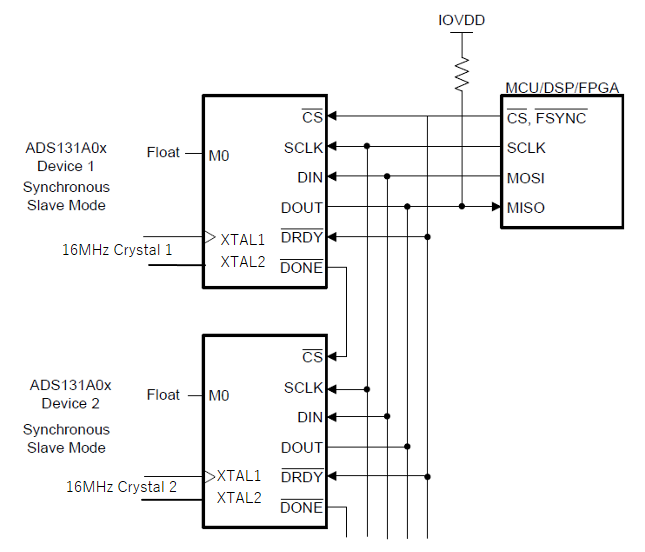
    The circuit is like this, "Fig 100. Multiple Device Configuration Using Synchronous Slave Mode".
    The two ADCs are connected in slave mode, and the clock sources are connected to different 16MHz crystal.
    The number of input channels to ADC1 and ADC2 is three channels.

    Logic signal in this connection is like this. And i think ADC devices and MPU communicating without probrem.

    Status response when asking ADC value is like this.

    Register Name Adress ADC device 1 ADC device 2
    STAT_1 0x02 0x14 0x14
    STAT_P 0x03 0x0C 0x0F
    STAT_N 0x04 0x0C

    0x0F

    STAT_S 0x05 0x00

    0x00

    ERROR_CNT 0x06 0x00

    0x00

    STAT_M2 0x07 0x06

    0x06

    Also the logic analyzer screen is not of Saleae. UI is similar with Saleae, but it's Kingst's LA1010.
    I have Saleae, but for now i can use Kingst La1010 or Analog Discovery 2.

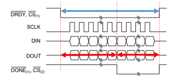
    I have a quesiton. Which is the correct definition of ”synchronization” in the timing diagram? Blue line or red line? Which signal should it be 7.812kHz?

  • Kenji-san,


    First, I received another question on E2E that is similar to something you mention in your last post. Here a link to that thread:

    https://e2e.ti.com/support/data-converters/f/73/t/894982

    Read through that post, and see what I wrote. As I mentioned in that post, I don't think you can get devices with two different clocks to work with one device in synchronous slave mode. Out of curiosity, are you working with this field applications engineer?

    For now, let's continue working on this with just looking at the communication. My thought was that the first device in asynchronous interrupt mode should still be giving data, even if the second device is not being synchronized properly.

    When I asked about the command response, I wasn't asking about the STAT register contents, I was asking about the command response for each command that you send it. For example, when you send the RESET, you should get the READY response at the beginning of the next frame. When you send the UNLOCK command, then you should see 0655h in the next frame and so on. This is shown with the commands and then the responses in Table 13 on page 48 of the datasheet. If you look through the initialization sequence, you can see if there are any bad responses from the commands. This could tell you if there is a bad initialization.

    In your last question, you asked about the synchronization. The synchronization from the device in asynchronous interrupt mode comes from the /DRDY line. This line from the first ADC tells the other ADC in synchronous slave mode when adc conversion completes. For the second device, this is an input into the /DRDY line.


    Joseph Wu

  • Joseph Wu-san

    Hi.

    I want use "Multiple Device Configuration Using Synchronous Slave Mode" .
    I want to be able to solve the problem that unable to get AD conversion value.

    I think TI has a schematic that verifies "Multiple Device Configuration Using Synchronous Slave Mode".
    Is it possible to show it?
    Also i want see the timing signals of SPI / DRDY / DONE actually measured by an oscilloscope or a logic analyzer at  "Multiple Device Configuration Using Synchronous Slave Mode". Of course, please also tell me the settings at that time.

    The quickest way to solve my problem is to look at the correct way TI did. And you have it. 
    I don't spend a lot of time, so please show the circuit diagram and actual timing signal data.

    Also we  have confirmed that it works even with another clock source  in ”Multiple Device Configuration Using Asynchronous Interrupt Mode”.

  • Kenji-san,


    I looked into the setup that we used to validate the device and I'm not sure that it will help. The schematic uses jumper connections to set up the connections needed for all the modes of operation. We did most of the characterization in asynchronous interrupt mode. However, we did run devices in both synchronous slave mode and synchronous master mode with the same board. Additionally, we used some custom FPGA programming to run the devices and collect data. I was not able to find the code use to run it. At this point, I don't have the boards or software to run the devices in synchronous slave mode. All I have is a schematic of the board that was used to characterize the device, and it was done so that it could accommodate all modes of operation.

    I would note that many customers have run multiple devices in some sort of synchronous mode, so I am confident that we can get it working as well.

    At this point, I still would like to see the command responses. I've also been thinking that we should definitely use a common master clock. without a common master clock, I don't think it's possible to get the clocks synchronized enough to work. Note the first device running in asynchronous interrupt mode generates the timing for the device running in synchronous slave mode.


    Joseph Wu

  • Joseph-san

    Now i working on async interrupt mode.
    And i could get AD value from the sensors.
    For now i connect with separate 16MHz crystal for CLKIN.

    I know the same CLKIN is the best solution for drive the ADC.
    So, to sync ADCs I ordered CDCLVC1102.
    Until CDCLVC1102 arrives, i will use crystal oscillator.