This thread has been locked.

If you have a related question, please click the "Ask a related question" button in the top right corner. The newly created question will be automatically linked to this question.

PCM3070 SPI problems

Other Parts Discussed in Thread: PCM3070

Hello all,

I made my own prototype board, using a PCM3070 connected with a MSP340 via a spi bus. I checked the signals of the spi, and they look ok using an oscilloscope. The problem is that pcm3070 don't confirm the data after being written with the MISO.

I checked voltage, and grounding. All are ok.

What could be the trouble?

Thank's you in advance

ip

  • Hi Ignasi,

    Pin 12 is the SPI_ SELECT pin, this determines if I2C or SPI communication is used. If this pin is high it will be in SPI mode, if low then it will be in I2C mode. What setting do you have this pin at?

    Justin
  • Hello Justin,

    SPI_SELECT is 1.

    Thank's for your help,
  • In case it helps, here I join the code of my msp430, trying to communicate unsuccesfully with the pcm3070

    //!                  MSP430F5259
    //!                 -----------------
    //!            /|\ |                 |
    //!             |  |                 |
    //!    Master---+->|RST              |
    //!                |             P1.4|-> Clock out to PCM3070 MCLK
    //!                |                 |
    //!                |             P1.6|-> LDO_SELECT
    //!                |                 |
    //!                |             P2.0|-> Reset PCM3070. Activated at "L"
    //!                |                 |
    //!                |             P2.1|-> SPI "H" or I2C "L"
    //!                |                 |
    //!                |             P2.2|-> Data Out (UCB3SIMO)
    //!                |                 |
    //!                |             P2.3|<- Data In (UCB3SOMI)
    //!                |                 |
    //!                |             P2.4|-> Serial Clock Out (UCB3CLK)
    //!                |                 |
    //!                |             P2.5|-> Chip Select Signal (UCB3STE)
    //!                |                 |
    //!                 -----------------
    
    //#include <msp430.h>
    
    #include <msp430f5259.h>
    #include "string.h"
    #include "stdio.h"
    
    /*#include "si446x_defs.h"
    #include "radio.h"
    #include "radio_config.h"
    #include "board.h"
    #include "si446x_api_lib.h"
    
    #include "radio_hal.h"*/
    
    #include "driverlib.h" //earplug
    
    #define SPICLK		500000
    #define TIMER_PERIOD 511
    #define DUTY_CYCLE  350
    
    uint8_t transmitData = 0x00, receiveData = 0x00; //earplug
    uint8_t returnValue = 0x00; //earplug
    uint8_t dataIndex = 0x00, dataIndex_Byte = 0x00;
    uint8_t TX_DATA[24][2] = {
    		{0x00,0x00},
    		{0x01,0x01},
    		{0x0b,0x81},
    		{0x0c,0x82},
    		{0x0d,0x00},
    
    		{0x0e,0x80},
    		{0x1b,0x10},
    		{0x3c,0x08},
    		{0x00,0x01},
    		{0x01,0x08},
    
    		{0x02,0x00},
    		{0x7b,0x01},
    		{0x14,0x25},
    		{0x0a,0x00},
    		{0x0c,0x08},
    
    		{0x0d,0x08},
    		{0x03,0x00},
    		{0x04,0x00},
    		{0x10,0x00},
    		{0x11,0x00},
    
    		{0x09,0x30},
    		{0x00,0x00},
    		{0x3f,0xd6},
    		{0x40,0x00}
    };
    
    //#ifdef 0
    //8.4KHz
    
    void main(void)
    {
        //Stop WDT
        WDT_A_hold(WDT_A_BASE);
    
        //SPI
        //Hardware reset slave PCM3070
        GPIO_setOutputLowOnPin(
            GPIO_PORT_P2,
            GPIO_PIN0
            );
    	__delay_cycles(5);
        //Hardware reset slave PCM3070 end
        GPIO_setOutputHighOnPin(
            GPIO_PORT_P2,
            GPIO_PIN0
            );
    	__delay_cycles(1000);
        //PCM3070 SPI selection at High State
        GPIO_setOutputHighOnPin(
            GPIO_PORT_P2,
            GPIO_PIN1
            );
    
        //PCM3070 LDO selection
        GPIO_setOutputLowOnPin(
            GPIO_PORT_P1,
            GPIO_PIN6
            );
    
        //P3.5,4,0 option select
        GPIO_setAsPeripheralModuleFunctionInputPin(
            GPIO_PORT_P2,
            GPIO_PIN2 + GPIO_PIN3 + GPIO_PIN4 + GPIO_PIN5
            );
    
    //#ifdef 1
        //TIMER
        //P1.4 as PWM output TA0.3
        GPIO_setAsPeripheralModuleFunctionOutputPin(
            GPIO_PORT_P1,
            GPIO_PIN4
            );
    
        //Generate PWM - Timer runs in Up mode
        TIMER_A_outputPWMParam param = {0};
        param.clockSource = TIMER_A_CLOCKSOURCE_SMCLK;
        param.clockSourceDivider = TIMER_A_CLOCKSOURCE_DIVIDER_1;
        param.timerPeriod = TIMER_PERIOD;
        param.compareRegister = TIMER_A_CAPTURECOMPARE_REGISTER_3;
        param.compareOutputMode = TIMER_A_OUTPUTMODE_RESET_SET;
        param.dutyCycle = DUTY_CYCLE;
        TIMER_A_outputPWM(TIMER_A0_BASE, &param);
    //#endif
    
        //SPI
        USCI_B_SPI_initMasterParam paramSPI = {0};
    	paramSPI.selectClockSource = USCI_B_SPI_CLOCKSOURCE_SMCLK;
    	paramSPI.clockSourceFrequency = UCS_getSMCLK();
    	paramSPI.desiredSpiClock = SPICLK;
    	paramSPI.msbFirst = USCI_B_SPI_MSB_FIRST;
    	paramSPI.clockPhase = USCI_B_SPI_PHASE_DATA_CHANGED_ONFIRST_CAPTURED_ON_NEXT;
    	paramSPI.clockPolarity = USCI_B_SPI_CLOCKPOLARITY_INACTIVITY_HIGH;
    	returnValue = USCI_B_SPI_initMaster(USCI_B3_BASE, &paramSPI);
    
    	if(STATUS_FAIL == returnValue)
    	{
    		return;
    	}
    
    	//Enable SPI module
    	USCI_B_SPI_enable(USCI_B3_BASE);
    
    	//Enable Receive interrupt
    	USCI_B_SPI_clearInterruptFlag(USCI_B3_BASE, USCI_B_SPI_RECEIVE_INTERRUPT);
    	USCI_B_SPI_enableInterrupt(USCI_B3_BASE, USCI_B_SPI_RECEIVE_INTERRUPT);
    
    	//Wait for slave to initialize
    	__delay_cycles(100);
    
    	//Initialize data values
    	transmitData = 0x00;
    
    	//USCI_A0 TX buffer ready?
    	while(!USCI_B_SPI_getInterruptStatus(USCI_B3_BASE,
    										 USCI_B_SPI_TRANSMIT_INTERRUPT))
    	{
    		;
    	}
    
    	//Transmit Data to slave
    	USCI_B_SPI_transmitData(USCI_B3_BASE, transmitData);
    //#endif
    
        //Enter LPM0, enable interrupts
        __bis_SR_register(LPM0_bits + GIE);
    
        //For debugger
        __no_operation();
    }
    
    //******************************************************************************
    //
    //This is the USCI_B0 interrupt vector service routine.
    //
    //******************************************************************************
    #if defined(__TI_COMPILER_VERSION__) || defined(__IAR_SYSTEMS_ICC__)
    #pragma vector=USCI_B3_VECTOR
    __interrupt
    #elif defined(__GNUC__)
    __attribute__((interrupt(USCI_B3_VECTOR)))
    #endif
    void USCI_B3_ISR(void)
    {
        switch(__even_in_range(UCB3IV,4))
        {
        //Vector 2 - RXIFG
        case 2:
            //USCI_A0 TX buffer ready?
            while(!USCI_B_SPI_getInterruptStatus(USCI_B3_BASE,
                                                 USCI_B_SPI_TRANSMIT_INTERRUPT))
            {
                ;
            }
    
            receiveData = USCI_B_SPI_receiveData(USCI_B3_BASE);
    
            //TRANSMISSION
            //Byte1
            if(dataIndex < 24)
            	transmitData = TX_DATA[dataIndex][0]; //Increment data index
            else
            	transmitData = 0x00;
            USCI_B_SPI_transmitData(USCI_B3_BASE,
                                    transmitData
                                    );		//Send next value
            __delay_cycles(40);		//Delay between transmissions for slave to process information
            //Byte2
            if(dataIndex < 24)
            	transmitData = TX_DATA[dataIndex][1]; //Increment data index
            else
            	transmitData = 0x00;
            USCI_B_SPI_transmitData(USCI_B3_BASE,
                                    transmitData
                                    );		//Send next value
            __delay_cycles(40);		//Delay between transmissions for slave to process information
    
            if(dataIndex < 24)
            {
    			//dataIndex_Byte++;
    			//if(dataIndex_Byte > 1)
    			//{
    				dataIndex++;
    			//	dataIndex_Byte = 0;
    			//}
            }
    
            break;
        default: break;
        }
    }

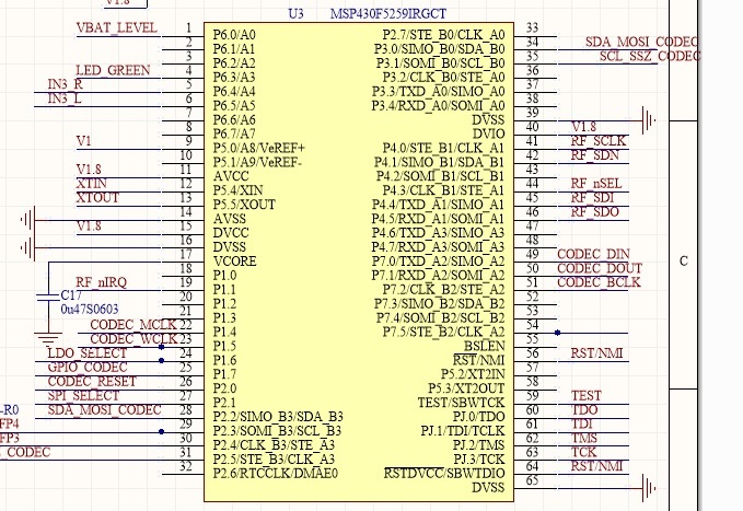
  • And the codec pcm3070 is connected with this schematics :

  • And the microcontroller . I cannot make them to communicate properly.

  • Hi Ignasi,

    It seems you are setting the SSZ pin as an input on the MSP430, this pin must be driven to let the PCM3070 know when SPI communication is coming. Please read section 2.7.2 in www.ti.com/.../slau332.pdf

    Justin
  • Hello Justin!

    Thank's for your help. After another reading again the section 2.7.2 it is clear for me that ssz must be driven. The problem I have right now, It is I don't know how to implement it on my code. Could you help me on this? A simple GPIO_setOutputHighOnPin() should work? If so, where should I implement it?

    I changed the port to output with the function GPIO_setAsPeripheralModuleFunctionOutputPin(), but it still doesn't work. Any other bugs?

    Thank you all for you help,

    ip

  • Hi Ignasi,

    The application document states:
    "The SSZ pin can remain low between transmissions; however, the PCM3070 only interprets the first 8 bits transmitted after the falling edge of SSZ as a command byte, and the next 8 bits as a data byte only if writing to a register."

    So you need to create a falling edge on the SSZ line at the start of every transmission.

    Justin

  • Dear Justin,

    So in the code below, how should I create the falling edge on the ssz line?
    //PCM3070 SPI SS
    GPIO_setOutputLowOnPin(GPIO_PORT_P2, GPIO_PIN5);

    But it doesn't act as a falling edge. Where should this line be?

    Thank's you a lot in advance.

    Best Regards

    ip
  • Dear Justin,

    So in the code below, how should I create the falling edge on the ssz line? Now I have the following line, but it doesn't drive.

    //PCM3070 SPI SS

     GPIO_setOutputLowOnPin(GPIO_PORT_P2, GPIO_PIN5);

    //!                  MSP430F5259
    //!                 -----------------
    //!            /|\ |                 |
    //!             |  |                 |
    //!    Master---+->|RST              |
    //!                |             P1.4|-> Clock out to PCM3070 MCLK
    //!                |                 |
    //!                |             P1.6|-> LDO_SELECT to "L"
    //!                |                 |
    //!                |             P2.0|-> Reset PCM3070. Activated at "L"
    //!                |                 |
    //!                |             P2.1|-> SPI "H" or I2C "L"
    //!                |                 |
    //!                |             P2.2|-> Data Out (UCB3SIMO)
    //!                |                 |
    //!                |             P2.3|<- Data In (UCB3SOMI)
    //!                |                 |
    //!                |             P2.4|-> Serial Clock Out (UCB3CLK)
    //!                |                 |
    //!                |             P2.5|-> Chip Select Signal (UCB3STE)
    //!                |                 |
    //!                 -----------------
    
            /*
             * Configure as SPI master mode.
             * Clock phase select, polarity, msb
             * UCMST = Master mode
             * UCSYNC = Synchronous mode
             * UCMODE_0 = 3-pin SPI
             */
    		 
    /*        HWREG8(baseAddress + OFS_UCBxCTL0) |= (
                    param->msbFirst +
                    param->clockPhase +
                    param->clockPolarity +
                    UCMST +
                    UCSYNC +
                    UCMODE_0
                    );
    */


    //#include <msp430.h>
    
    #include <msp430f5259.h>
    
    #include "string.h"
    #include "stdio.h"
    
    #include "driverlib.h" //earplug
    
    #define SPICLK		25000
    #define TIMER_PERIOD 4
    #define DUTY_CYCLE  2
    
    uint8_t transmitData = 0x00, receiveData = 0x00; //earplug
    uint8_t returnValue = 0x00; //earplug
    uint8_t dataIndex = 0x00, dataIndex_Byte = 0x00;
    uint8_t TX_DATA[24][2] = {
    		{0x00,0x00},
    		{0x01,0x01},
    		{0x0b,0x81},
    		{0x0c,0x82},
    		{0x0d,0x00},
    
    		{0x0e,0x80},
    		{0x1b,0x10},
    		{0x3c,0x08},
    		{0x00,0x01},
    		{0x01,0x08},
    
    		{0x02,0x00},
    		{0x7b,0x01},
    		{0x14,0x25},
    		{0x0a,0x00},
    		{0x0c,0x08},
    
    		{0x0d,0x08},
    		{0x03,0x00},
    		{0x04,0x00},
    		{0x10,0x00},
    		{0x11,0x00},
    
    		{0x09,0x30},
    		{0x00,0x00},
    		{0x3f,0xd6},
    		{0x40,0x00}
    };
    
    void main(void)
    {
        //Stop WDT
        WDT_A_hold(WDT_A_BASE);
        //Set Outputs
        GPIO_setAsOutputPin(
    		GPIO_PORT_P2,
    		GPIO_PIN0 + GPIO_PIN1 + GPIO_PIN5
        );
    
        GPIO_setAsOutputPin(
            GPIO_PORT_P1,
            GPIO_PIN6
            );
    
        //SPI
        //Hardware reset slave PCM3070
        GPIO_setOutputLowOnPin(
            GPIO_PORT_P2,
            GPIO_PIN0
            );
    
        //PCM3070 SPI selection at High State
        GPIO_setOutputHighOnPin(
            GPIO_PORT_P2,
            GPIO_PIN1
            );
    
        //PCM3070 LDO selection to Low
        GPIO_setOutputLowOnPin(
            GPIO_PORT_P1,
            GPIO_PIN6
            );
    
        //P3.5,4,0 option select
        GPIO_setAsPeripheralModuleFunctionInputPin(
            GPIO_PORT_P2,
            GPIO_PIN2 + GPIO_PIN3 + GPIO_PIN4
            );
    
        //PCM3070 SPI SS
        GPIO_setOutputHighOnPin(
            GPIO_PORT_P2,
            GPIO_PIN5
            );
        //P3.5,4,0 option select
        //GPIO_setAsPeripheralModuleFunctionOutputPin(
        //    GPIO_PORT_P2,
        //    GPIO_PIN5
        //    );
    
    //#ifdef 1
        //TIMER
        //P1.4 as PWM output TA0.3
        GPIO_setAsPeripheralModuleFunctionOutputPin(
            GPIO_PORT_P1,
            GPIO_PIN4
            );
    
        //Generate PWM - Timer runs in Up mode
        TIMER_A_outputPWMParam param = {0};
        param.clockSource = TIMER_A_CLOCKSOURCE_SMCLK;
        param.clockSourceDivider = TIMER_A_CLOCKSOURCE_DIVIDER_1;
        param.timerPeriod = TIMER_PERIOD;
        param.compareRegister = TIMER_A_CAPTURECOMPARE_REGISTER_3;
        param.compareOutputMode = TIMER_A_OUTPUTMODE_RESET_SET;
        param.dutyCycle = DUTY_CYCLE;
        TIMER_A_outputPWM(TIMER_A0_BASE, &param);
    //#endif
    
        //SPI
        USCI_B_SPI_initMasterParam paramSPI = {0};
    	paramSPI.selectClockSource = USCI_B_SPI_CLOCKSOURCE_SMCLK;
    	paramSPI.clockSourceFrequency = UCS_getSMCLK();
    	paramSPI.desiredSpiClock = SPICLK;
    	paramSPI.msbFirst = USCI_B_SPI_MSB_FIRST;
    	paramSPI.clockPhase = USCI_B_SPI_PHASE_DATA_CHANGED_ONFIRST_CAPTURED_ON_NEXT;
    	paramSPI.clockPolarity = USCI_B_SPI_CLOCKPOLARITY_INACTIVITY_LOW;
    	returnValue = USCI_B_SPI_initMaster(USCI_B3_BASE, &paramSPI);
    
    	if(STATUS_FAIL == returnValue)
    	{
    		return;
    	}
    
    	//Enable SPI module
    	USCI_B_SPI_enable(USCI_B3_BASE);
    
    	//Enable Receive interrupt
    	USCI_B_SPI_clearInterruptFlag(USCI_B3_BASE, USCI_B_SPI_RECEIVE_INTERRUPT);
    	USCI_B_SPI_enableInterrupt(USCI_B3_BASE, USCI_B_SPI_RECEIVE_INTERRUPT);
    
        //Now with SPI signals initialized, reset slave
        GPIO_setOutputHighOnPin(
            GPIO_PORT_P2,
            GPIO_PIN0
            );
    
    	//Wait for slave to initialize
    	__delay_cycles(1000);
    
    	//Initialize data values
    	transmitData = 0x00;
    
    	//USCI_A0 TX buffer ready?
    	while(!USCI_B_SPI_getInterruptStatus(USCI_B3_BASE,
    										 USCI_B_SPI_TRANSMIT_INTERRUPT))
    	{
    		;
    	}
        //PCM3070 SPI SS
        GPIO_setOutputLowOnPin(GPIO_PORT_P2, GPIO_PIN5);
    
    	//Transmit Data to slave
    	USCI_B_SPI_transmitData(USCI_B3_BASE, transmitData);
    //#endif
    
        //PCM3070 SPI SS
        GPIO_setOutputHighOnPin(GPIO_PORT_P2, GPIO_PIN5);
    
        //Enter LPM0, enable interrupts
        __bis_SR_register(LPM0_bits + GIE);
    
        //For debugger
       // __no_operation();
    }
    
    //******************************************************************************
    //
    //This is the USCI_B0 interrupt vector service routine.
    //
    //******************************************************************************
    #if defined(__TI_COMPILER_VERSION__) || defined(__IAR_SYSTEMS_ICC__)
    #pragma vector=USCI_B3_VECTOR
    __interrupt
    #elif defined(__GNUC__)
    __attribute__((interrupt(USCI_B3_VECTOR)))
    #endif
    void USCI_B3_ISR(void)
    {
        switch(__even_in_range(UCB3IV,4))
        {
        //Vector 2 - RXIFG
        case 2:
            //USCI_B3 TX buffer ready?
            while(!USCI_B_SPI_getInterruptStatus(USCI_B3_BASE,
                                                 USCI_B_SPI_TRANSMIT_INTERRUPT))
            {
                ;
            }
    
            receiveData = USCI_B_SPI_receiveData(USCI_B3_BASE);
    
            //TRANSMISSION
            //Byte1
            if(dataIndex < 24)
            	transmitData = TX_DATA[dataIndex][0]; //Increment data index
            else
            	transmitData = 0x00;
    
            //PCM3070 SPI SS
            GPIO_setOutputLowOnPin(GPIO_PORT_P2, GPIO_PIN5);
            USCI_B_SPI_transmitData(USCI_B3_BASE,
                                    transmitData
                                    );		//Send next value
            //PCM3070 SPI SS
    	    GPIO_setOutputHighOnPin(GPIO_PORT_P2, GPIO_PIN5);
            __delay_cycles(40);		//Delay between transmissions for slave to process information
    
            //Byte2
            if(dataIndex != 0)
            {
    			if(dataIndex < 24)
    				transmitData = TX_DATA[dataIndex][1]; //Increment data index
    			else
    				transmitData = 0x00;
    		    //PCM3070 SPI SS
    		    GPIO_setOutputLowOnPin(GPIO_PORT_P2, GPIO_PIN5);
    			USCI_B_SPI_transmitData(USCI_B3_BASE,
    									transmitData
    									);		//Send next value
    		    //PCM3070 SPI SS
    		    GPIO_setOutputHighOnPin(GPIO_PORT_P2, GPIO_PIN5);
    			__delay_cycles(40);		//Delay between transmissions for slave to process information
            }
    
            if(dataIndex < 24)
            {
    			//dataIndex_Byte++;
    			//if(dataIndex_Byte > 1)
    			//{
    				dataIndex++;
    			//	dataIndex_Byte = 0;
    			//}
            }
    
            break;
        default: break;
        }
    }
    

  • (this code still doesn't work on spi )
  • Hi Ignasi,

    Have you checked the SPI output with a sniffer to verify the MSP430 is outputting the correct values? Do you have the PCM3070 EVM? If so you could use the GUI to talk over SPI and use a sniffer and compare the GUI/EVM output to your custom setup.

    For detailed support on the MSP430 code you will have to head over to the MSP430 forum : e2e.ti.com/.../166

    Justin
  • Hello Justin,

    Thank's for your help.

    I can check using an oscilloscope, that clk from spi is ok, and mosi got some data travelling throught it. On the other hand, miso is always blocked to 1. Unfortunatly, I don't have pcm3070 evm, so I couldn't do the sniffing over gui.

    I have chosen this product after using it on a evm c5517, but on this case, we were running on I2C and worked good using the example. If you have any other idea, please tell me. I would be very glad to find the bug!

    Best regards

    ip
  • Hi IP,

    What is the behavior of the slave select line?

    Justin
  • Hello Justin,

    Unfortunatly, I don't have access to ste. 

    I'm exploring a new option, sending a communication package to my pcm3070 requesting an answer, to see if it's dead or not. But I couldn't find any example about it in spi. Right now, to be honest, I'm so lost I don't know what else to do.

    Thank you for your help in advance

    ip

  • //!                  MSP430F5259
    //!                 -----------------
    //!            /|\ |                 |
    //!             |  |                 |
    //!    Master---+->|RST              |
    //!                |             P1.4|-> Clock out to PCM3070 MCLK
    //!                |                 |
    //!                |             P1.6|-> LDO_SELECT to "L"
    //!                |                 |
    //!                |             P2.0|-> Reset PCM3070. Activated at "L"
    //!                |                 |
    //!                |             P2.1|-> SPI "H" or I2C "L"
    //!                |                 |
    //!                |             P2.2|-> Data Out (UCB3SIMO)
    //!                |                 |
    //!                |             P2.3|<- Data In (UCB3SOMI)
    //!                |                 |
    //!                |             P2.4|-> Serial Clock Out (UCB3CLK)
    //!                |                 |
    //!                |             P2.5|-> Chip Select Signal (UCB3STE)
    //!                |                 |
    //!                 -----------------
    
            /*
             * Configure as SPI master mode.
             * Clock phase select, polarity, msb
             * UCMST = Master mode
             * UCSYNC = Synchronous mode
             * UCMODE_0 = 3-pin SPI
             */
    		 
    /*        HWREG8(baseAddress + OFS_UCBxCTL0) |= (
                    param->msbFirst +
                    param->clockPhase +
                    param->clockPolarity +
                    UCMST +
                    UCSYNC +
                    UCMODE_0
                    );
    */


    //#include <msp430.h>
    
    #include <msp430f5259.h>
    
    #include "string.h"
    #include "stdio.h"
    
    #include "driverlib.h" //earplug
    
    #define SPICLK		25000
    #define TIMER_PERIOD 4
    #define DUTY_CYCLE  2
    
    uint8_t transmitData = 0x00, receiveData = 0x00; //earplug
    uint8_t returnValue = 0x00; //earplug
    uint8_t dataIndex = 0x00, dataIndex_Byte = 0x00;
    uint8_t TX_DATA[24][2] = {
    		{0x00,0x00},
    		{0x01,0x01},
    		{0x0b,0x81},
    		{0x0c,0x82},
    		{0x0d,0x00},
    
    		{0x0e,0x80},
    		{0x1b,0x10},
    		{0x3c,0x08},
    		{0x00,0x01},
    		{0x01,0x08},
    
    		{0x02,0x00},
    		{0x7b,0x01},
    		{0x14,0x25},
    		{0x0a,0x00},
    		{0x0c,0x08},
    
    		{0x0d,0x08},
    		{0x03,0x00},
    		{0x04,0x00},
    		{0x10,0x00},
    		{0x11,0x00},
    
    		{0x09,0x30},
    		{0x00,0x00},
    		{0x3f,0xd6},
    		{0x40,0x00}
    };
    
    void main(void)
    {
        //Stop WDT
        WDT_A_hold(WDT_A_BASE);
        //Set Outputs
        GPIO_setAsOutputPin(
    		GPIO_PORT_P2,
    		GPIO_PIN0 + GPIO_PIN1 + GPIO_PIN5
        );
    
        GPIO_setAsOutputPin(
            GPIO_PORT_P1,
            GPIO_PIN6
            );
    
        //SPI
        //Hardware reset slave PCM3070
        GPIO_setOutputLowOnPin(
            GPIO_PORT_P2,
            GPIO_PIN0
            );
    
        //PCM3070 SPI selection at High State
        GPIO_setOutputHighOnPin(
            GPIO_PORT_P2,
            GPIO_PIN1
            );
    
        //PCM3070 LDO selection to Low
        GPIO_setOutputLowOnPin(
            GPIO_PORT_P1,
            GPIO_PIN6
            );
    
        //P3.5,4,0 option select
        GPIO_setAsPeripheralModuleFunctionInputPin(
            GPIO_PORT_P2,
            GPIO_PIN2 + GPIO_PIN3 + GPIO_PIN4
            );
    
        //PCM3070 SPI SS
        GPIO_setOutputHighOnPin(
            GPIO_PORT_P2,
            GPIO_PIN5
            );
        //P3.5,4,0 option select
        //GPIO_setAsPeripheralModuleFunctionOutputPin(
        //    GPIO_PORT_P2,
        //    GPIO_PIN5
        //    );
    
    //#ifdef 1
        //TIMER
        //P1.4 as PWM output TA0.3
        GPIO_setAsPeripheralModuleFunctionOutputPin(
            GPIO_PORT_P1,
            GPIO_PIN4
            );
    
        //Generate PWM - Timer runs in Up mode
        TIMER_A_outputPWMParam param = {0};
        param.clockSource = TIMER_A_CLOCKSOURCE_SMCLK;
        param.clockSourceDivider = TIMER_A_CLOCKSOURCE_DIVIDER_1;
        param.timerPeriod = TIMER_PERIOD;
        param.compareRegister = TIMER_A_CAPTURECOMPARE_REGISTER_3;
        param.compareOutputMode = TIMER_A_OUTPUTMODE_RESET_SET;
        param.dutyCycle = DUTY_CYCLE;
        TIMER_A_outputPWM(TIMER_A0_BASE, &param);
    //#endif
    
        //SPI
        USCI_B_SPI_initMasterParam paramSPI = {0};
    	paramSPI.selectClockSource = USCI_B_SPI_CLOCKSOURCE_SMCLK;
    	paramSPI.clockSourceFrequency = UCS_getSMCLK();
    	paramSPI.desiredSpiClock = SPICLK;
    	paramSPI.msbFirst = USCI_B_SPI_MSB_FIRST;
    	paramSPI.clockPhase = USCI_B_SPI_PHASE_DATA_CHANGED_ONFIRST_CAPTURED_ON_NEXT;
    	paramSPI.clockPolarity = USCI_B_SPI_CLOCKPOLARITY_INACTIVITY_LOW;
    	returnValue = USCI_B_SPI_initMaster(USCI_B3_BASE, &paramSPI);
    
    	if(STATUS_FAIL == returnValue)
    	{
    		return;
    	}
    
    	//Enable SPI module
    	USCI_B_SPI_enable(USCI_B3_BASE);
    
    	//Enable Receive interrupt
    	USCI_B_SPI_clearInterruptFlag(USCI_B3_BASE, USCI_B_SPI_RECEIVE_INTERRUPT);
    	USCI_B_SPI_enableInterrupt(USCI_B3_BASE, USCI_B_SPI_RECEIVE_INTERRUPT);
    
        //Now with SPI signals initialized, reset slave
        GPIO_setOutputHighOnPin(
            GPIO_PORT_P2,
            GPIO_PIN0
            );
    
    	//Wait for slave to initialize
    	__delay_cycles(1000);
    
    	//Initialize data values
    	transmitData = 0x00;
    
    	//USCI_A0 TX buffer ready?
    	while(!USCI_B_SPI_getInterruptStatus(USCI_B3_BASE,
    										 USCI_B_SPI_TRANSMIT_INTERRUPT))
    	{
    		;
    	}
        //PCM3070 SPI SS
        GPIO_setOutputLowOnPin(GPIO_PORT_P2, GPIO_PIN5);
    
    	//Transmit Data to slave
    	USCI_B_SPI_transmitData(USCI_B3_BASE, transmitData);
    //#endif
    
        //PCM3070 SPI SS
        GPIO_setOutputHighOnPin(GPIO_PORT_P2, GPIO_PIN5);
    
        //Enter LPM0, enable interrupts
        __bis_SR_register(LPM0_bits + GIE);
    
        //For debugger
       // __no_operation();
    }
    
    //******************************************************************************
    //
    //This is the USCI_B0 interrupt vector service routine.
    //
    //******************************************************************************
    #if defined(__TI_COMPILER_VERSION__) || defined(__IAR_SYSTEMS_ICC__)
    #pragma vector=USCI_B3_VECTOR
    __interrupt
    #elif defined(__GNUC__)
    __attribute__((interrupt(USCI_B3_VECTOR)))
    #endif
    void USCI_B3_ISR(void)
    {
        switch(__even_in_range(UCB3IV,4))
        {
        //Vector 2 - RXIFG
        case 2:
            //USCI_B3 TX buffer ready?
            while(!USCI_B_SPI_getInterruptStatus(USCI_B3_BASE,
                                                 USCI_B_SPI_TRANSMIT_INTERRUPT))
            {
                ;
            }
    
            receiveData = USCI_B_SPI_receiveData(USCI_B3_BASE);
    
            //TRANSMISSION
            //Byte1
            if(dataIndex < 24)
            	transmitData = TX_DATA[dataIndex][0]; //Increment data index
            else
            	transmitData = 0x00;
    
            //PCM3070 SPI SS
            GPIO_setOutputLowOnPin(GPIO_PORT_P2, GPIO_PIN5);
            USCI_B_SPI_transmitData(USCI_B3_BASE,
                                    transmitData
                                    );		//Send next value
            //PCM3070 SPI SS
    	    GPIO_setOutputHighOnPin(GPIO_PORT_P2, GPIO_PIN5);
            __delay_cycles(40);		//Delay between transmissions for slave to process information
    
            //Byte2
            if(dataIndex != 0)
            {
    			if(dataIndex < 24)
    				transmitData = TX_DATA[dataIndex][1]; //Increment data index
    			else
    				transmitData = 0x00;
    		    //PCM3070 SPI SS
    		    GPIO_setOutputLowOnPin(GPIO_PORT_P2, GPIO_PIN5);
    			USCI_B_SPI_transmitData(USCI_B3_BASE,
    									transmitData
    									);		//Send next value
    		    //PCM3070 SPI SS
    		    GPIO_setOutputHighOnPin(GPIO_PORT_P2, GPIO_PIN5);
    			__delay_cycles(40);		//Delay between transmissions for slave to process information
            }
    
            if(dataIndex < 24)
            {
    			//dataIndex_Byte++;
    			//if(dataIndex_Byte > 1)
    			//{
    				dataIndex++;
    			//	dataIndex_Byte = 0;
    			//}
            }
    
            break;
        default: break;
        }
    }
    

    I enclose to you the last version of my code :

  • Last update, now I don't have signals at all outside my msp430. No bus, no clock..
  • Hi Ignasi,

    It seems you need to verify your SPI operation on the MSP430. You can head over to the MSP430 forum on E2E for help with getting SPI working.

    Justin
  • Hello Justin,

    Thank's for your help.

    After your first recommendation on the MSP430 forum, I created a post with all the documentacion on the problem, and my advances. Unfortunatly, I couldn't have any answer on the topic.

    Best Regards

    ip

  • Hello Justin,

    Thank's for your help. 

    Could you please confirm me that you don't see any design problem on the PCM3070? Voltage, Grounding, Capacities.... In case it doesn't work because a wrong wiring...

    Thank you in advance!

    ip

  • Hi IP,

    I have looked over the schematic again and I have a few comments:

    -many of the mode select pins are driven by the MSP430, so making sure they are set correctly with a probe when testing could be helpful. (along with the SS pin)
    -You are supplying AVDD with VBAT, is this a regulated supply?
    -I don't see any filtering on the input, only DC blocking caps, unless there are filters elsewhere.

    Everything else looks good.

    Justin
  • Hello Justin,

    Thank's again for your support.

    - I have tested the selected pins driven by MSP430, and they are all ok, related to configuration.

    - AVdd is a regulated supply. On my case, regulated 1.8V

    - Filters are on another part of the design. On the board, they are close to codec.

    I couldn't have any help on MSP340 forum. From my side, I just had some advances, I could see my spi signals on oscilloscope, so spi is alive. The thing is I try to configure a single beep on the outside, to confirm it is alive. But I couldn't. With my actual spi bus I still cannot program the registers. Maybe spi parameters are wrong?

    UCB3CTL1 |= UCSWRST; // **Put state machine in reset**
    UCB3CTL0 |= UCMST+UCSYNC+UCCKPL+UCMSB; // 3-pin, 8-bit SPI master
    // Clock polarity high, MSB
    UCB3CTL1 |= UCSSEL_2; // SMCLK
    UCB3BR0 = 0x02;///0x02; // /2
    UCB3BR1 = 0; //
    UCA0MCTL = 0; // No modulation. Just needed on UCA0, no on ucb3
    UCB3CTL1 &= ~UCSWRST; // **Initialize USCI state machine**
    UCB3IE |= UCRXIE+UCTXIE; // Enable USCI_B3 RX interrupt

    Working with the Clock on 8 MHz.

    The configuration of the codec, pretending to have a Beep on the output LOL is the following :

    ///codec_spi_w_r_byte(unsigned char Reg_Address, unsigned char w_r, unsigned char data)


    codec_spi_w_r_byte( 0, 0, 0x00); // Select page 0
    codec_spi_w_r_byte( 1, 0, 0x01); // Reset codec
    codec_spi_w_r_byte( 0, 0, 0x01); // Point to page 1
    codec_spi_w_r_byte( 1, 0, 0x08); // Disable crude AVDD generation from DVDD
    codec_spi_w_r_byte( 2, 0, 0x00); // Enable Analog Blocks
    /* PLL and Clocks config and Power Up */
    codec_spi_w_r_byte( 0, 0, 0x00); // Select page 0
    codec_spi_w_r_byte( 27, 0, 0x00); // BCLK and WCLK is set as i/p to AIC3204(Slave}
    codec_spi_w_r_byte( 4, 0, 0x00); // PLL setting: PLLCLK <- BCLK and CODEC_CLKIN <-PLL CLK
    codec_spi_w_r_byte( 6, 0, 0x20); // PLL setting: J=32
    codec_spi_w_r_byte( 7, 0, 0x00); // PLL setting: HI_BYTE(D = 0}
    codec_spi_w_r_byte( 8, 0, 0x00); // PLL setting: LO_BYTE(D} = 0
    /* For 48 KHz sampling */
    codec_spi_w_r_byte( 5, 0, 0x92); // PLL setting: Power up PLL, P=1 and R=2
    codec_spi_w_r_byte( 13, 0, 0x00); // Hi_Byte(DOSR} for DOSR = 128 decimal or 0x0080 DAC oversamppling
    codec_spi_w_r_byte( 14, 0, 0x80); // Lo_Byte(DOSR} for DOSR = 128 decimal or 0x0080
    codec_spi_w_r_byte( 20, 0, 0x80); // AOSR for AOSR = 128 decimal or 0x0080 for decimation filters 1 to 6
    codec_spi_w_r_byte( 11, 0, 0x88); // Power up NDAC and set NDAC value to 8
    codec_spi_w_r_byte( 12, 0, 0x82); // Power up MDAC and set MDAC value to 2
    codec_spi_w_r_byte( 18, 0, 0x88); // Power up NADC and set NADC value to 8
    codec_spi_w_r_byte( 19, 0, 0x82); // Power up MADC and set MADC value to 2

    /* DAC ROUTING and Power Up */

    codec_spi_w_r_byte( 0, 0, 0x1); // Select page 1
    codec_spi_w_r_byte( 14, 0, 0x08); // LDAC AFIR routed to LOL
    codec_spi_w_r_byte( 15, 0, 0x08); // RDAC AFIR routed to LOR
    codec_spi_w_r_byte( 0, 0, 0x00); // Select page 0
    codec_spi_w_r_byte( 64, 0, 0x02); // Left vol=right vol
    codec_spi_w_r_byte( 65, 0, 0x00); // Left DAC gain to 0dB VOL, Right tracks Left
    codec_spi_w_r_byte( 63, 0, 0xd4); // Power up left,right data paths and set channel
    codec_spi_w_r_byte( 0, 0, 0x01); // Select page 1
    codec_spi_w_r_byte( 18, 0, 0x06); // Unmute LOL , 6dB gain
    codec_spi_w_r_byte( 19, 0, 0x06); // Unmute LOR , 6dB gain
    codec_spi_w_r_byte( 9, 0, 0x30); // Power up HPL,HPR
    codec_spi_w_r_byte( 0, 0, 0x00); // Select page 0

    /* ADC ROUTING and Power Up */
    codec_spi_w_r_byte( 0, 0, 0x1); // Select page 1
    codec_spi_w_r_byte( 51, 0, 0x08); // SetMICBIAS
    codec_spi_w_r_byte( 52, 0, 0x08); // STEREO 1 Jack

    codec_spi_w_r_byte( 55, 0, 0x04); // IN3_L to LADC_P through 40 kohm
    // IN3_R to RADC_P through 40 kohmm
    codec_spi_w_r_byte( 54, 0, 0x03); // CM_1 (common mode} to LADC_M through 40 kohm
    codec_spi_w_r_byte( 57, 0, 0xc0); // CM_1 (common mode} to RADC_M through 40 kohm
    codec_spi_w_r_byte( 59, 0, 0x5f); // MIC_PGA_L unmute
    codec_spi_w_r_byte( 60, 0, 0x5f); // MIC_PGA_R unmute
    codec_spi_w_r_byte( 0, 0, 0x00); // Select page 0
    codec_spi_w_r_byte( 81, 0, 0xc0); // Powerup Left and Right ADC
    codec_spi_w_r_byte( 82, 0, 0x00); // Unmute Left and Right ADC


    codec_spi_w_r_byte( 0, 0, 0x00); // Select page 0
    codec_spi_w_r_byte( 48, 0, 0x04); // Beep Generator
    codec_spi_w_r_byte( 52, 0, 0x14);
    codec_spi_w_r_byte( 0, 0, 0x00) ; // Select page 0

    I'm also afraid, if code is ok, but configuration is not good and I cannot know where the codec is...

    Best Regards and Thank's for your help

    ip

  • Here the information on filtering stage :

  • Hi IP,

    I believe there is a difference in meaning between SPI settings in the MSP430 documentation and the PCM3070 definitions. Try changing the following code:

    From:
    UCB3CTL0 |= UCMST+UCSYNC+UCCKPL+UCMSB; // 3-pin, 8-bit SPI master

    To this:
    UCB3CTL0 |= UCMST+UCSYNC+UCMSB; // 3-pin, 8-bit SPI master

    If this does not correct the SPI communication I would suggest using the EVM and using your script through one of our GUIs to test the script itself without the complication of the SPI communication.

    Justin