This thread has been locked.

If you have a related question, please click the "Ask a related question" button in the top right corner. The newly created question will be automatically linked to this question.

DIX9211 sampling frequency calculator

Other Parts Discussed in Thread: DIX9211, SRC4392, PCM1792, PCM1792A, DSD1794A, SN74LVC157A, DSD1792A

Hi

The DIX9211 looks very flexible. Especially the multichannel routing function and the input / output sampling frequency calculators are very interesting.

I have a question based on my experience with Wolfson's WM8805 s/pdif receiver which i have used so far. It indicates (of course in software operation mode) only four recovered frequencies: 32KHz, 44.1 or 48KHz, 88.2 or 92KHz and 192KHz. That is a very rough indication and the 176.4KHz is not included. Also, its Input Channel Status registers are out of order. For that reason i decided to replace it.

DIX9211 can realy indicate all sampling frequencies as is stated in the manual through the relevant i/o calculators?

Another one question is that: It is worthy to i turn in SRC4392 instead DIX9211? I know a bit the benefits of async. sampling rate conversion. The only that bothers me is that, if we inject a DSD signal the SRC4392 will pass it to the SRC converter which is desirable only for PCM signals. Whilst DIX9211 does not includes a SRC converter and so is suitable to accept and route either PCM or DSD input signals at its I2S output. In the case of SRC4392 i think for DSD we have to use an external multiplexer before the DAC and i don't like it because i fear for jitter issues.

What do you think about that?

Thanks

Fotis    

  • Hi Fotis,

    The DIX9211 has a register value for 15 different sampling rates that it can detect from 8 kHz to 192 kHz. This is shown in the register map of the data sheet page on page 73 and 74. The DIX9211 can identify each of these sampling rates.

    When using the SRC4392 you can choose whether a signal is passed through the SRC or not. So if your DSD data will work over normal PCM pass through, then you can do so on the SRC4392.

    Justin
  • Hi Justin

    Many thanks for the reply.

    Now i am turned to SRC4392, it is a fantastic chip. My question remains the same regarding bypass the SRC when DSD data are injected. OK, for the case of DSD data over PCM (or DoP) your reply seems to be correct. There are PC media players like JRiver and Foobar which can convert a DSD datastream in DoP. I forgot to refer that i will use a USB 2.0 Audio interface (e.g. of XMOS or something simillar) of which the same data lines are shared between PCM (I2S) and DSD formats. These lines will be connected at the "Audio Serial Port A" of SRC4392. The issue is that: there are music files which are offered in native DSD format on web stores. If the user does not use the JRiver media player to convert the native DSD file in DoP (believe me, there are many DSD audio or "Pulse Density Modulation" fans out there) then the 4392 could bypass its internal sampling rate converter to directly drive the native DSD data at the output i.e. the "Audio Serial Port B"?

    That is my question as well my assumption that in case of native DSD audio data only an external MUX could bypass the SRC.

    Can you enlighten me please on this issue?

    Thank you very much

    Fotis       

  • Hi Fotis,

    I will have to look more into the behavior when DSD is input to port A. I will post when I have more information.

    Justin
  • Thank you so much Justin
    Your information and.... maybe your side of view will be precious. I haven't someone to discuss these difficult issues.

    Regards

    Fotis
  • Hi Fotis,

    Have you looked at using an I2S switch to switch around the SRC part when DSD is being output? This would allow a single source to output to the SRC input and the switch input 1. The other input of the switch, input 2, would be the SRC output. The output of the switch would then go to the receiver of the I2S/DSD data. The switch would be a SN74**244, any of these parts could work.

    Justin

  • Hi Justin

    Thank you very much for the advice and your time

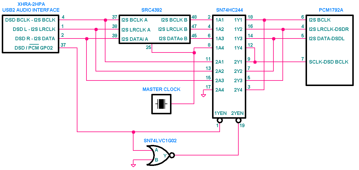
    I think what you suggest is shown in the following block diagram

    The only that bothers me is that the Master Clock for which my plan is to use a high quality 24.576MHz TCXO instead the provided clock by the PCM or S/PDIF streams, it is necessary to pass through the HC244. It is an issue of PCM1792 as it shares the same pin for both the System Clock and DSD Bit Clock inputs. 

    There is also the option of use of HC157A (Quad 2-Input Data Selector/Multiplexer) instead HC244. The beneffit (?) is that there is no need of connecting-shorting the output pins of the two separate quad switches 1Ax and 2Ax. What do you think about it?  

    Any last comment will be appreciated.

    Thank you again

    Fotis

  • Hi Fotis,

    The HC157A might be a better solution, as you could set up the inputs to switch to the correct signals for DSD or PCM to the corresponding pin on the PCM1792A. I would think the crystal would still be in the same position of having to split into to inputs.\

    Justin
  • Hi Justin

    Thank you for the advice.

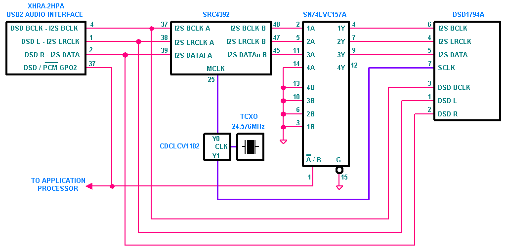
    I think that i found a solution for a clean way for Master Clock. We simply have to replace the PCM1792A with its brother DSD1794A. This DAC offers the same performance like PCM1792A, I2C control, but separate inputs for PCM and DSD. Take a look on the schematic below:

    The MCLK lines are represented with magenta. The TCXO feeds the CDCLCV1102 clock buffer which in sequence shares the MCLK to both SRC4392 and DSD1794A directly without any interface. Super!

    The only issue (but of minor importance) is that: when the DSD mode is asserted, the PCM (I2S) inputs of DSD1794A must be grounded. According this, the use of multiplexer SN74LVC157A seems to be necessary.

    When the USB2 Audio interface detects a DSD data stream, forces in HI state its GPO2 output pin 37. Accordingly the grounded "B" inputs of SN74LVC157A (1B, 2B, 3B) are connected to its "Y" outputs (1Y, 2Y, 3Y), thus driving the PCM inputs of DSD1794A in LOW state.

    Tell me please your thought about this implementation.

    Many thanks

    Regards

    Fotis

  • Hi Fotis,

    You could also use the DSD1792A which would be software controlled while the DSD1794A is hardware controlled. Since you only need a way to stop the output of the SRC you can jut use a 4 gate AND IC and have an enable signal go to the other side of the AND gate. You could also eliminate the need for the gate and you can power down the SRC output and the outputs will be forced low. This can be done in register 0x01.

    Justin
  • Hi Justin

    Thank you for the reply and the advice. 

    Regarding the output of SRC, your advice to power down it is brilliant as i didn't knew it that its outputs are forced LOW. This will save me from one chip!

    Regarding DSD1794A, although in the main page and in the header description inside quotes is refered (H/W control), in the further description as well inside the manual is clearly refered as I2C controlled. There are schematics, instructions etc within the pdf doc in which is shown the I2C control mode process. So which of the two is the true? H/W or S/W controlled? Can you check please the page of DSD1794A to confirm?

    As for the DSD1792A it looks just fine, simply i don't like  the SPI software control because it consumes 4 pins from the application MCU whilst I2C only two.

    Thank you again

    Fotis 

  • As Justin replied to my other post:

    The DSD1794A is a software controlled device. The control protocol offered is only I2C.

    Regards

    Fotis