This thread has been locked.

If you have a related question, please click the "Ask a related question" button in the top right corner. The newly created question will be automatically linked to this question.

TLV320AIC3262 register settings

Other Parts Discussed in Thread: TLV320AIC3262

Hi,

I receive a question about the TLV320AIC3262 register settings from a customer. By a certain setting, TVL320AIC3262 does not output sound from HPR. I show an example of the failure of register setting.

figure 1


figure 2
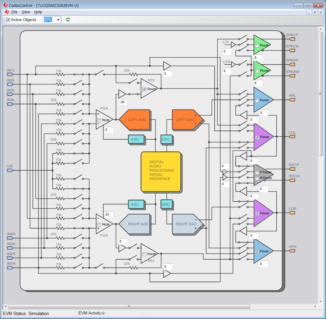

Figure 1 is a setting the LEFT DAC signal outputs from RECP/M, and figure 2 is a setting the LEFT DAC signal outputs from HPR. Sometimes HPR does not output a sound when changing the path from figure 1 to figure 2. In this case, before the figure 2 setting, by addition to some register settings as shown below, HPR could output a sound.

B0_P0_R0 = 0x01
B0_P1_R27 = 0x03
B0_P1_R28 = 0x00
B0_P1_R31 = 0x80

However he can't insert these register settings because of software structure and lack of micro-controller resources. Is there any way of register settings to prevent the failure of HPR output? Up to now, HPL outputs a sound by similar setting. An example of setting is as follows.

B0_P0_R0 = 0x00
B0_P0_R127 = 0x00
B0_P0_R0 = 0x01
B0_P1_R55 = 0x00
B0_P1_R57 = 0x00
B0_P0_R0 = 0x00
B0_P0_R81 = 0x02
B0_P0_R82 = 0xc8
B0_P0_R0 = 0x04
B0_P4_R86 = 0x0c
B0_P0_R0 = 0x01
B0_P1_R52 = 0x00
B0_P1_R18 = 0x3f
B0_P1_R22 = 0x04
B0_P1_R36 = 0x38
B0_P1_R17 = 0x00
B0_P0_R0 = 0x00
B0_P0_R63 = 0x00
B0_P0_R0 = 0x01
B0_P1_R40 = 0x00
B0_P1_R40 = 0x39
B0_P0_R0 = 0x00
B0_P0_R64 = 0x0c

################ additional settings ################

*B0_P0_R0 = 0x01
*B0_P1_R27 = 0x03
*B0_P1_R28 = 0x00
*B0_P1_R31 = 0x80

#####################################################

B0_P0_R0 = 0x01
B0_P1_R59 = 0x80
B0_P1_R60 = 0xb0
B0_P1_R122 = 0x05
B0_P1_R51 = 0x3a
B0_P1_R58 = 0x00
B0_P0_R0 = 0x04
B0_P4_R10 = 0x01
B0_P0_R0 = 0x00
B0_P0_R19 = 0x30
B0_P0_R12 = 0x08
B0_P0_R11 = 0x02
B0_P0_R6 = 0x11
B0_P0_R6 = 0x91
B0_P0_R11 = 0x82
B0_P0_R19 = 0xb0
B0_P0_R12 = 0x88
B0_P0_R0 = 0x01
B0_P1_R51 = 0x7e
B0_P1_R58 = 0xff
B0_P0_R0 = 0x04
B0_P4_R10 = 0x00
B0_P0_R0 = 0x01
B0_P1_R122 = 0x01
B0_P1_R59 = 0x00
B0_P1_R60 = 0x30
B0_P0_R0 = 0x00
B0_P0_R81 = 0x42
B0_P0_R0 = 0x01
B0_P1_R55 = 0x01
B0_P1_R57 = 0x40
B0_P0_R0 = 0x00
B0_P0_R82 = 0xc0
B0_P0_R0 = 0x04
B0_P4_R87 = 0x0d
B0_P0_R0 = 0x01
B0_P1_R52 = 0xc0
B0_P1_R18 = 0x28
B0_P1_R22 = 0x87
B0_P1_R17 = 0x08
B0_P0_R0 = 0x00
B0_P0_R63 = 0x80
B0_P0_R0 = 0x01
B0_P1_R27 = 0x01
B0_P0_R0 = 0x00
B0_P0_R65 = 0x04
B0_P0_R0 = 0x01
B0_P1_R29 = 0x00
B0_P1_R32 = 0x00
B0_P0_R0 = 0x00
B0_P0_R64 = 0x04
B0_P0_R0 = 0x01
B0_P1_R28 = 0x7f
B0_P1_R31 = 0xb9

Best regards,
Akio Ito

  • Hi, Ito-san,

    I will take a look at this and I will answer as soon as possible.

    Best regards,
    Luis Fernando Rodríguez S.
  • Luis-san,

    Thanks for your reply. I am waiting for your answer.

    Best regards,
    Akio Ito

  • Ito-san,

    I already reviewed the register configuration. It seems that the additional settings must be used to generate the headphone output. Could you describe the customer limitations for this case, please? I mean, is it possible to add these lines at the end of the code? (See the following line codes as example)

    B0_P0_R0 = 0x01
    B0_P1_R27 = 0x03
    B0_P1_R28 = 0x00
    B0_P1_R31 = 0x80
    B0_P1_R27 = 0x01
    B0_P1_R28 = 0x7f
    B0_P1_R31 = 0xb9

    Best regards,
    Luis Fernando Rodríguez S.
  • Luis-san,

    Thanks for your answer. I will ask to him whether it is possible to add those lines at the end of the code. But the reply will be late. Because most of Japanese workers have holidays from tomorrow until the end of next week. I cannot get his answer until the holiday is over.

    Best regards,
    Akio Ito

  • Ito-san,

    Thank you for your response. I will be waiting for the answer.

    Best regards,
    Luis Fernando Rodríguez S.
  • Luis-san,

    I received another question from my customer. He let the ADC and DAC power down to enter the device into standby mode. However sometimes the ADC and DAC flags did not power down. The TLV320AIC3262 register configuration for standby mode referred to slaa473b is as follows.

    Standby Modes Configuration

    1a. Configure amplifier gains to -6dB
    Register(s):
    b0_p1_r31_b5-0 = 111010b (HPL = -6dB, unmute)
    b0_p1_r32_b5-0 = 111010b (HPR = -6dB, unmute)
    b0_p1_r40_b5-0 = 111010b (RECP = -6dB, unmute)
    b0_p1_r41_b5-0 = 111010b (RECM = -6dB, unmute)
    b0_p1_r48_b6-4 = 001b (SPKL = 6dB, unmute)
    b0_p1_r48_b2-0 = 001b (SPKR = 6dB, unmute)
    b0_p1_r28_b6-0 = 1110101b (LOL to HPL = -78.3 dB, unmute)
    b0_p1_r29_b6-0 = 1110101b (LOR to HPR = -78.3 dB, unmute)
    b0_p1_r36_b6-0 = 1110101b (LOL to RECP = -78.3 dB, unmute)
    b0_p1_r37_b6-0 = 1110101b (LOR to RECM = -78.3 dB, unmute)
    b0_p1_r46_b6-0 = 1110101b (LOL to SPKL = -78.3 dB, unmute)
    b0_p1_r47_b6-0 = 1110101b (LOR to SPKR = -78.3 dB, unmute)
    Flag(s):
    b0_p1_r63_b7 (HPL gain flag)
    b0_p1_r63_b6 (HPR gain flag)
    b0_p1_r63_b5 (RECP gain flag)
    b0_p1_r63_b4 (RECM gain flag)
    b0_p1_r64_b7 (LOL to HPL gain flag)
    b0_p1_r64_b7 (LOR to HPR gain flag)
    b0_p1_r64_b6 (LOL to RECP gain flag)
    b0_p1_r64_b5 (LOR to RECM gain flag)
    b0_p1_r64_b4 (LOL to SPKL gain flag)
    b0_p1_r64_b3 (LOR to SPKR gain flag)

    1b. Power down internal amplifiers
    Register(s):
    b0_p1_r31_b5-0 = 111001b (HPL = mute)
    b0_p1_r32_b5-0 = 111001b (HPR = mute)
    b0_p1_r40_b5-0 = 111001b (RECP = mute)
    b0_p1_r41_b5-0 = 111001b (RECM = mute)
    b0_p1_r17_b3-2 = 00b (power down MAL/MAR)
    b0_p1_r22_b1-0 = 00b (power down LOL/LOR)
    b0_p1_r27_b1-0 = 00b (power down HPL/HPR)
    b0_p1_r40_b7-6 = 00b (power down RECP/RECM)
    b0_p1_r45_b1-0 = 00b (power down SPKL/SPKR)
    Flag(s):
    b0_p1_r66_b7 (LOL power status)
    b0_p1_r66_b6 (LOR power status)
    b0_p1_r66_b5 (HPL power status)
    b0_p1_r66_b4 (HPR power status)
    b0_p1_r66_b3 (RECP power status)
    b0_p1_r66_b2 (RECM power status)
    b0_p1_r66_b1 (SPKL power status)
    b0_p1_r66_b0 (SPKR power status)

    1c. Configure MicPGA
    Register(s):
    b0_p1_r59_b7 = 1b (set to 0dB Left MICPGA Gain)
    b0_p1_r60_b7 = 1b (set to 0dB Right MICPGA Gain)
    b0_p1_r52_b7-0 = 00000000b (MicPGA_LP routing)
    b0_p1_r53_b5-4 = 00b ()
    b0_p1_r54_b7-0 = 00000000b (MicPGA_LM routing)
    b0_p1_r55_b7-0 = 00000000b (MicPGA_RP routing)
    b0_p1_r56_b5-4 = 00b ()
    b0_p1_r57_b7-0 = 00000000b (MicPGA_RM routing)

    2b. Set reference to forced mode
    Register(s):
    b0_p1_r122_b2 = 1b (forced REF power-up)

    3. Disable AGCs
    Register(s):
    b0_p0_r87_b5-1 = 00000b (disable LAGC noise threshold)
    b0_p0_r95_b5-1 = 00000b (disable RAGC noise threshold)
    b0_p0_r86_b7 = 0b (disable LAGC)
    b0_p0_r94_b7 = 0b (disable RAGC)

    4. Power down ADCs
    Register(s):
    b0_p0_r81_b7-6 = 00b (power down both ADCs)
    Flag(s):
    b0_p0_r36_b6 (LADC power status)
    b0_p0_r36_b2 (RADC power status)

    5. Power down DACs
    Register(s):
    b0_p0_r63_b7-6 = 00b (power down both DACs)
    Flag(s):
    b0_p0_r37_b7 (LDAC power status)
    b0_p0_r37_b3 (RDAC power status)

    6. Disconnect output amplifier routing
    Register(s):
    b0_p1_r23_b7 = 0b (MAL output is not routed to LOL driver)
    b0_p1_r23_b6 = 0b (MAR output is not routed to LOR driver)
    b0_p1_r23_b4-3 = 0b (IN1L input is not routed to LOL driver)
    b0_p1_r23_b1-0 = 0b (IN1R input is not routed to LOR driver)
    b0_p1_r27_b7 = 0b (MAL output is not routed to HPL driver)
    b0_p1_r27_b6 = 0b (MAR output is not routed to HPR driver)
    b0_p1_r27_b5 = 0b (Left DAC is not routed to HPL driver)
    b0_p1_r27_b4 = 0b (Right DAC is not routed to HPR driver)

    7. Power off additional blocks
    Register(s):
    b0_p1_r51_b6 = 0b (power down MICBIAS_EXT)
    b0_p1_r51_b2 = 0b (power down MICBIAS)
    b0_p1_r58_b7-0 = 00000000b (disable weak bias for all inputs)
    b0_p4_r10_b0 = 1b (disable forced audio serial interface output)
    b0_p4_r12_b7 = 0b (power off BCLK N divider)
    b0_p0_r22_b7 = 0b (power off CLKOUT M divider)
    b0_p0_r67_b7 = 0b (disable headset detection for sleep mode)

    8. Power down clock generation tree
    Register(s):
    b0_p0_r19_b7 = 0b (power down MADC divider)
    b0_p0_r12_b7 = 0b (power down MDAC divider)
    b0_p0_r18_b7 = 0b (power down NADC divider)
    b0_p0_r11_b7 = 0b (power down NDAC divider)
    b0_p0_r6_b7 = 0b (power down PLL)


    Best regards,
    Akio Ito
  • Luis-san,

    I got my customer's response to your suggestion. He said it seemed to have no problem. This problem was resolved thanks to your support.
    Sorry, I had transmitted the same contents twice by mistake. But would you cooperate with us about the next problem too?

    Best regards,
    Akio Ito

  • Hello, Ito-san,

    I'm glad to read that the first problem was solved.

    Regarding the flags issue, the ADCs and DACs are not powered down immediately. So, the ADC/DAC flags could take some time to be powered down. Could customer add a delay before read the ADC/DAC flags, please? Could customer try with 1us?

    Please let me know if the problem persists.

    Best regards,
    Luis Fernando Rodríguez S.
  • Luis-san,

    I'm sorry for the delayed response. He is testing your suggestion now. And he has two questions.
    Q1. Should the next register setting do after confirming the ADC/DAC power down flags?
    Q2. He chose MCLK as a clock source of ADC/DAC. Can the power down flags read even if MCLK stops?
     
    Best regards,
    Akio Ito

  • Hello, Ito-san,

    Q1. Should the next register setting do after confirming the ADC/DAC power down flags?
    Correct. It is important to verify that the ADC/DAC power down flags are enabled in order to continue with the register configuration.

    Q2. He chose MCLK as a clock source of ADC/DAC. Can the power down flags read even if MCLK stops?
    There are few functions of the codec that cannot be made without the MCLK. All the registers related with the ADC and DAC need a MCLK working. So, the power down flags need the MCLK too.

    Best regards,
    Luis Fernando Rodríguez S.
  • Luis-san,

    Thanks for your answer. Because of a hardware restriction, he seems to begin a standby mode sequence after stop of the MCLK.
    Is there any means to avoid it?

    Best regards,
    Akio Ito

  • Ito-san,

    The MCLK can be stopped once the device is on standby mode. The standby mode doesn't require MCLK pulses since the ADC/DAC is disabled.

    Best regards,
    Luis Fernando Rodríguez S.