This thread has been locked.

If you have a related question, please click the "Ask a related question" button in the top right corner. The newly created question will be automatically linked to this question.

TLV320AIC3268 Evaluation / interface with a MCU

Other Parts Discussed in Thread: TLV320AIC3268, TLV320AIC34, TLV320DAC3203, TLV320DAC3101

Hello

I Have to evaluate the TLV320AIC3268 CODEC.

I bougth the TLV320AIC3268EVM-U evaluation board, downloaded PPC2 and began testing with some scripts.

Now, I want to interface a MCU to the CODEC,to evaluate the ADC / DAC interface, this way:

- still using the PPC2 to configure the CODEC with the I2C port

- connect BCLK1, WCLK1, DIN1 and DOUT1 to the serial interface of the MCU in TDM or DSP format

I tested different scripts, but I still have a 44.1 kHz clock on the WCLK1 output (on TP8) while using the script 6.2 (for instance) which should lead to: the following

Clock configuration

MCLK = 4.096 MHz, BCLK = 512 kHz, WCLK = 8 kHz (slave)

After what, every script I tested returns the same result (44.1kHz clock on WCLK1).

Could you please indicate me what is the issue? Is there any HW modification? jumper configuration? register configuration.. to do what I want

Many thanks.

Regards

Stéphane


I I j

  • Hi, Stephane,

    Welcome to E2E and thank you for your interest in our products!

    In general, our codec EVMs receive the I2S clocks from another U2B-to-I2S controller. This EVM uses the TAS1020B to generate the I2S clocks. When the codec is configured in master mode, these clocks must be disabled to avoid any collision from the TAS1020B I2S clocks and the AIC3268 I2S clocks. Also, the WCLK and BCLK must be configured as outputs.

    Could you disconnect the jumpers JP5 and JP6, please? This is to ensure that the BCLK1 and WCLK1 are not provided from the TAS1020B. Please take a look at the TLV320AIC3268EVM-U Schematic for details.

    Best regards,
    Luis Fernando Rodríguez S.

  • Hi Luis.

    Thanks for your response.

    Unfortunately I already did the test:

    - I disconnected JP5 + JP6

    - I used script 6.3 which uses the PLL to generate WCLK at 44.1 kHz

    But the WCLK1 signal (TP8) remains at the high level.

    Isn't there any issue with the GPIO1 which seems to be used as reference for the HF_CLKIN?

    Best regards

    Stéphane

  • Hi, Stéphane,

    WCLK and BCLK signals remains at high level for few reasons:

    - WCLK and BCLK are not configured as outputs.
    - MCLK is not being provided.
    - ADC/DAC are not powered up.
    - BCLK output is not enabled.

    Could you verify all these configurations?

    Best regards,
    Luis Fernando Rodríguez S.
  • Hi Luis

    I succeeded in generating WCLK, BCLK, and Data out

    I connected to a serial port of a MCU.

    The serial port is configured into DSP mode: a Frame synchro + 16 bits first word followed by a second 16 bits word.

    I used this to configure the ADC :

    #########################################################################################
    # Audio Input Configuration
    #########################################################################################
    w 30 00 01 # Select Page 1
    w 30 34 40 # LEFT_P = IN1L (10K)
    w 30 36 00 # LEFT_M = CM1L (10K)
    w 30 37 40 # RIGHT_P = IN1R (10K)
    w 30 39 00 # RIGHT_M = CM1R (10K)
    w 30 3b 00 # L_MicPGA = 0dB
    w 30 3c 00 # R_MicPGA = 0dB
    w 30 00 00 # Select Page 0
    w 30 51 c0 # Power up LADC/RADC
    w 30 52 00 # Unmute LADC/RADC

    And I applied sinus signal to IN1L TP25 on the evaluation board.

    Unfortunately the sampled signal is totally uncoherent..

    I need this for correct evaluation of the CODEC:

    input signal  --> ADC -> samples into the MCU + process --> Output to DAC to HP for example

    Could you give me some indication some tests to do to understand what is going wrong.

    I would be on vacations next 3 weeks, but I will have to work on it and solve it.

    Best regards and many thanks for your support.

    Stéphane

  • Hi, Stéphane,

    Could you give some details about the serial data interface of the AIC3268? Is it configured in DSP mode and 16-bits of word length? Do you have captures of the WCLK and BCLK generation?

    Thank you.

    Best regards,
    Luis Fernando Rodríguez S.
  • Hi Fernando

    Yes it is configured in DSP Mode, 16 bits length.

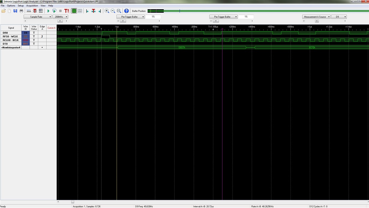
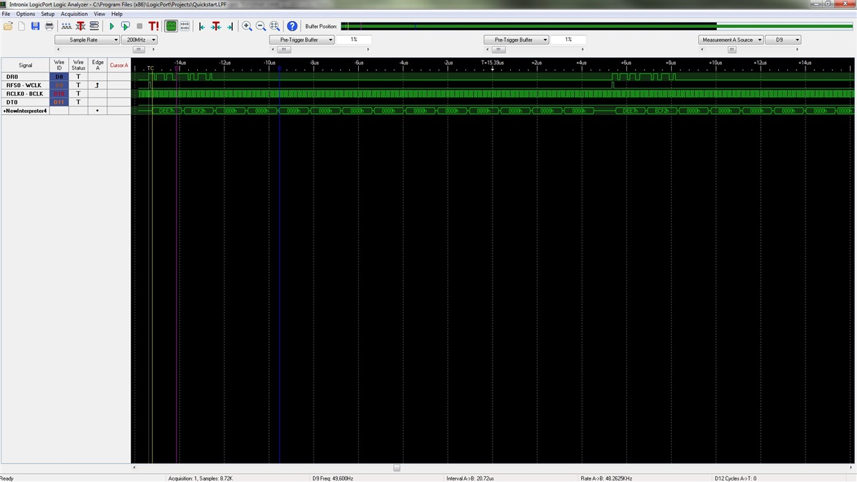
    These should have been two attached files of the capture of BCLK, WCLK, DR0, DT0 (not used for the moment).

    Thank you for your support.

    Best regards

    Stéphane CHARVIT

    I encountered isues for ataching files (trying to attach .jpg files I indicated the file, but it returned me an error) and the only non rejected way was to control paste from word, but I think it does not send the é wave forms. An other way?

  • Hi, Stéphane,

    You should be able to attach files with using the rich formatting (this option appear once you press the reply button). Regarding the I2S waveforms, are there differences in phase or level with the I2S signals of the EVM?

    Best regards,
    Luis Fernando Rodríguez S.
  • Hi Luis

    I had the rich formatting option after I pressed the reply button.

    I had then the same issue: I chose the file(s) to be transmitted) with the browser, afterwhat it begun transmitting (I suppose) and I have the error text in red which appeared beside of the name of the file.

    So, I am still unable to send you files..

    For the waveforms I don't understand your question. In fact I used the DSP Mode (8.3.9.2.4.4 paragraph of the data sheet), 16 bits, no offset.

    The TLV320AIC3268 Code is master and suplies the signals BCLK, WCLK, DOUT to the MCU.

    I used a logicp port to make acquisition of signals and I could see constant successive and maybe uncoherent samples values on Dout.

    I wonderer if I enter correctly the sgnal on the EVM or if correctly defined the audio input configuration in the script:

    #########################################################################################
    # Audio Input Configuration
    #########################################################################################
    w 30 00 01 # Select Page 1
    w 30 34 40 # LEFT_P = IN1L (10K)
    w 30 36 40 # LEFT_M = CM1L (10K)
    w 30 37 40 # RIGHT_P = IN1R (10K)
    w 30 39 40 # RIGHT_M = CM1R (10K)
    w 30 3b 00 # L_MicPGA = 0dB
    w 30 3c 00 # R_MicPGA = 0dB
    w 30 00 00 # Select Page 0
    w 30 51 c0 # Power up LADC/RADC
    w 30 52 00 # Unmute LADC/RADC

    I send a single ended signal on TP25, with JP3 on 1-2 position

    I have to fix this quickly to go on with evaluation: DAC part, multi channel configuration, DSP process, SAR utilization ....

    It should have been very usefull to be able to send attached files but I don't understand why I have an error when I tried..

    Thank you for your support

    Best regards

    Séphane CHARVIT

  • I finally succeded in transmitting the files..

    Sory , it was from my side ..

    Best regards

    Stéphane CHARVIT

  • Hi, Stéphane,

    Thank you for provide the pictures.

    I would like to compare the data serial interface clocks when you use the MCU and when you don't use it. I mean, the TLV320AIC3268EVM generates the I2S signals from the TAS1020b. You mentioned that the EVM is working correctly until you use your MCU. This means that the problem is related with the data transmission between the MCU and the EVM. So, which are the differences between the TAS1020b clocks and the MCU clocks? Could you compare the WCLKs, BCLKs and MCLKs of both cases?

    I hope to have been clear. Please let me know if you have questions or comments about this.

    Thank you.

    Best regards,
    Luis Fernando Rodríguez S.
  • Hi Luis,

    Thanks for helping.

    First, I don't know if the EVm is working totally properly or not, because I am evaluating it. In fact I want to use the fonctionnality and direct I2C interface with PC and PurePath Console to reprogramm esaily the CODEC. But at the same time I don't want the TAS1020b to interact with my tests.

    I mean:

    1) I programm the CODEC using th TI  supplied scripts I have modified

    2) I connect the serial interface from the TP: TP7 for BLCK, TP8 for WLCK, TP9 for DIN, and TP10 for DOUT to the PCB card of my MCU (in fact it is a DSP for the moment, any way ...)

    The signals are in DSP mode, 48kHz sample rate, 16 bits, L/R IN1 connected to ADC

    Then I run a specific code into my DSP to read the L/R samples and store them into a data array. I just store L or R ways samples. In this case I store just Right way.

    I send a (approx) 1V rms 1kHz signal to IN1R in TP27 through C89 with JP34 on 1-2 position

    The DSP software is running properly, sampling and receiving the data from the CODEC but the values are totally uncoherent. The DSP IS RECEIVING THE SIGNALS BCLK, WCLK, DOUT FROM THE CODEC AS A SLAVE.

    I was prety confident that the serial link is correctly running but the ADC not. Indeed when I made the acquisition with my Logic Port analyzer which supplied the traces I sent, I have the same uncoherent values on the Dout signal: data are not sinus (increasing or decreasing regularly) and are repetitive (sucessivec samples are equals.

    I wonder if this could come from the TAS1020B USB driver which could interfer or with the Common mode CM1L/R. When CM1L/R are activated I have the issue like if just sampling noise and when they are disabled I have just zeros.

    Is it possible to use the EVM this way or not? Is the TAS1020B is interfering with my test or not?

    Am I correctly programming the Audio Input interface, knowing I want to connect the input analogic signal to IN1/R?

    w 30 00 01 # Select Page 1
    w 30 34 40 # LEFT_P = IN1L (10K)
    w 30 36 40 # LEFT_M = CM1L (10K)
    w 30 37 40 # RIGHT_P = IN1R (10K)
    w 30 39 00 # RIGHT_M = CM1R (10K)
    w 30 3b 00 # L_MicPGA = 0dB
    w 30 3c 00 # R_MicPGA = 0dB
    w 30 00 00 # Select Page 0
    w 30 51 c0 # Power up LADC/RADC
    w 30 52 00 # Unmute LADC/RADC

    Best regards

    Stéphane CHARVIT

  • Hi, Stéphane,

    Thank you for the information that you provided.

    I suspect that this could be related with the TAS1020b. We need to ensure several things to properly get the data from the codec. In this case, you should ensure that the TAS1020b is not being connected to the codec.

    - You should ensure that jumpers related with the I2S clocks are not being connected from the TAS1020b to the AIC3268. This means that you should disconnect jumpers JP4 to JP8.

    - MCLK should be provided from your PCB board to have all clocks in phase. I mean, the codec should generate the BCLK and WCLK from the MCLK. This could be made with the help of the internal dividers or PLL (see Figure 58. Clock Distribution Tree for details).

    - The codec must be configured in master mode to make this. Ensure that BCLK and WCLK are generated correctly from the codec.

    Please let me know if the problem persists.

    Best regards,
    Luis Fernando Rodríguez S.

  • Hi Luis,

    Thanks a lot for your reponse.

    Indeed, I forgot to remove JP7 and JP8. I have already removed JP5 and JP6. Unfortunately it does not fix totally the issue

    But I don't think it is necessary to remove JP4. I think it is possible to use the MCLK from the EVM, then to generate BCLK and WCLK from it, using as you said, and as I did the internal dividers DOSR, AOSR. The DSP receives BCLK, WCLK and Data out from Codec as a slave and seems to be ok with that.

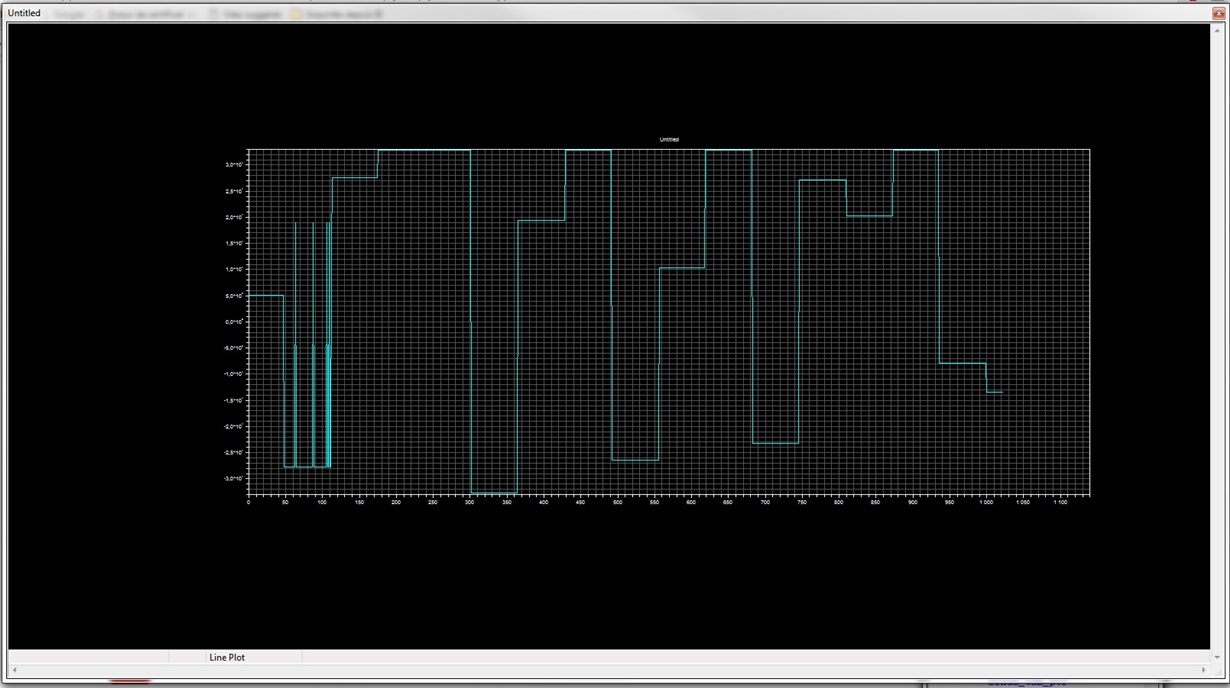
    Unfortunately the data output from the CODEC on DOUT1_DUT (TP10) seems to be wrong: repetitive values.

    I send you the screen directly aquired from a scope on TP10 (Dout is the blue trace, WCLK is the orange one)

     and the data received and stored in a circular buffer into the DSP:

    It seems the data are not evolving like the input sinus signal.

    The signal is read on TP27 at the IN1R entry and is a correct sinus signal:

    Is there a problem with the internal mapping?

    Best regards

    Stephane

  • Hi Luis,

    Good news!

    It is working correctly.

    In fact, as I wanted the ADC to work the same way and at the same frequency than the DAC, I set ADC_CLK = DAC CLK (w 30 12 00) and ADC_MOD_CLOCK = DAC_MOD_CLOCK (w 30 13 00)

    But this doesn not permit the AD C to be powered. That's why it was not working.
    So, I set, the same values for NADC than for NDAC and for MADC than for MDAC, and powered M and N ADC: w 30 12 81; NADC = 1, powered and w 30 13 82 MADC = 2, powered,

    With these values, it is working properly and I can go on with my evaluations tests.

    Thanks a lot for your support.

    Best regards

    Stéphane CHARVIT

    TELERAD, France

  • Hi, Stéphane,

    I'm glad to read that you solved this issue. Please let us know if you have more questions or comments in the future. We will be glad to help you.

    Best regards,
    Luis Fernando Rodríguez S.
  • Hi Luis

    I go on with the CODEC evaluation. May I go on this post or do I need to create a new subject?

    I need to process and generate a few analog signals.

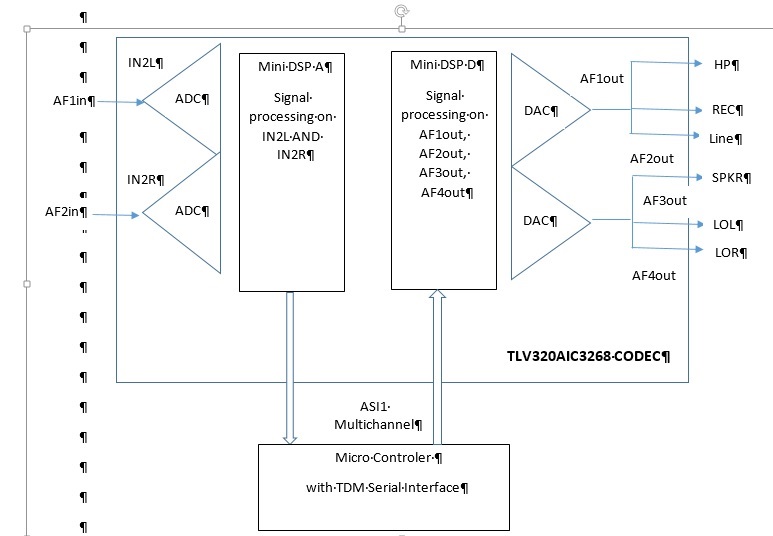
    This figure can illustrate what I need to do:

    Two analog Audio Frequencies signals AF1in and AF2in (single ended) are converted by the ADC. And is it possible to have AF3 and AF4 analog signals?
    Then they are processed by mini DSP A
    Then they are sent on ASI1 (Dout) to the host micro controller to be analyzed and processed.
    The processor generates AF1out, AF2out, AF3out, and AF4out and sent them on ASI1 Din to the mini DSP D for additional signal processing.
    Then, AF1out is converted by the DAC and output on HP, REC, and Line with different gains.
    AF2out is is converted by the DAC and output on SPKR.
    AF3out is is converted by the DAC and output on LOL.
    AF4out is is converted by the DAC and output on LOR.
    Is it possible to do such a process with the ALVAIC3268 CODEC?

    Or is it necessary to use additional components? It yes, could you, please recommend me any of these components reference (AD, DAC, digital amplifier, other?)
    Many thanks for your support
    Best regards
    Stéphane
     
     
  • Hi, Stéphane,

    In this case, there are several limitations that you should consider when using the TLV320AIC3268.

    The TLV320AIC3268 has two ADCs and two DACs. This means that the ADCs can be configured to receive one signal at time (AF1in for first ADC, AF2in for second ADC). So, your ADC inputs won't be a problem. However, the DACs will be able to support one signal at time. So, you should select two of your four outputs (AF1out, AF2out, AF3out, AF4out).

    The rest of your application will be possible if the microcontroller supports TDM mode. There are several multi_channel_digital_in/out blocks in PurePath Studio that you may use to configure the codec in an easier way.

    Please let me know if you have more questions or comments.

    Best regards,
    Luis Fernando Rodríguez S.
  • Hi Luis

    Once more, thank you for your response and clarifications.

    So If I understand correctly: AF1in and AF2in may be converted by the ADCs of the CODEC TLV320AIC3268.

    If I have more AFin, I have to find others ADCs.

    AF1out may be converted by DAC1 and sent on HP, REC, and Line.

    AF2out may be converted by DAC2 and sent on other output.

    AF3out and AF4out have to be converted by others DACs.

    Is there any DAC multichannel you could recommend?

    The CODEC TLV320AIC3268 could send data to be converted (AF3out an AF4out) using ASI3?

    Or is it preferable to use two TLV320AIC3268 CODECs?

    Thank you very much

    Best regards

    Stéphane CHARVIT

  • Hi, Stéphane,

    That's right. You would require of more ADCs and DACs in case you need more signals. Each of ADCs and DACs only support one signal. In this case, you only require of more DACs to reach your requirements.

    So, if you require a single chip solution, I would recommend the TLV320AIC34. This is single codec solution with two codecs in one. So, it supports four ADCs and four DACs. However, this codec doesn't have a great processing such the TLV320AIC3268. The TLV320AIC34 doesn't support miniDSP.

    If you only need additional DACs, you may use the TLV320DAC3101 or TLV320DAC3203.

    Best regards,
    Luis Fernando Rodríguez S.
  • Hi Luis

    I have others questions about the TLV320AIC 3268 CODEC:

    1°)

    I am begginnig to program with the Pure Path Studio the ambedded mini DSP of the CODEC.

    I have programmed a 96 TAPS FIR. I can see in the ressources window there is 65,23% of used mini_DSP_A_coeff1 words.

    If I want use others fir this is a limitation because this memory will be full and this leads to a build error.

    There is a mini_DSP_A_coeff0 memory area which is almost empty: 0,26% used. 

    Is it possible to use it and how to do to indicate we want the coeff to be stored in this memory area?

    2°)

    Using a mux: if we want to chnage the way we select, we have to write using the SPI/I2C interface at the right adress, is it true?

    3°) 

    using the output DAC:

    Is it possible to send the same DAC output to several outputs: for instance: Line, HP, and speaker, with different gains?

    How to do that?

    Many thanks for your answers.

    Best regards

    Stéphane

  • Hi, Stéphane,

    1) The blocks memory is assigned depending of the target processor. The target processor can be miniDSP_A or miniDSP_D. If you require to share memory between both miniDSPs, you may use an interprocessor block to modify the target processor from A to D or vice versa. Additionally, you may extend the memory resources if you disable the adaptive mode for both miniDSPs. However, if you disable this mode, you won't be able to modify the coefficients while the ADC/DAC is powered up.

    2) That's correct. You may take a look at the multiplexer help window. It explains how many bytes will be used to assign the channel. You would need to modify the correct address via SPI/I2C. The correct address is mentioned in Component _Interface section of Properties Window.

    3) That's right. You would need to modify the SystemSettingsCode of the AIC3268 Framework. This code modifies the register configuration. In case you require to route the DAC to several outputs, you would need to modify the DAC and outputs sections of this code.

    Please let me know if you have further questions or comments.

    Best regards,
    Luis Fernando Rodríguez S.
  • Hi Luis,

    Thank you for your responses.

    Just coming back on my first question.

    1°I wondered how to assign into one mini DSP into the coeff0 or into coeff1 memory area. If we focus on the mini DSP A, could you please tell me how to indicate to the builder hos to place coeff filters into mini_DSP_A_coeff0 rather than into mini_DSP_A_coeff1?

    Thanks a lot for the recommandation to disable the adaptative mode In our application we don't need to modify the filters coefficients. So it helps reducing efficeintly the used memory space.

    2°)

    An other question

    If we disable the adaptative mode, will it still be possible to modify the multiplexer select writting the correct address using the SPI interface?

    Because when we disable it is not possible enay more to modify it in the PurePath software whil in running mode.

    Many thanks for your support.

    Best regards

    Stéphane

  • Hi, Stéphane,

    The coefficients are assigned by PurePath Studio once the .pfw file is built. So, I recommend to open the Options Window of Tools Menu. You will find a Built Menu where you may modify the AIC Assambler options. I recommend to select "Optimize Coefficient Memory". This option will reduce your coefficient memory and, if possible, will distribute the coefficients in a better way.

    Best regards,
    Luis Fernando Rodríguez S.
  • Hi Luis

    We succeeded in developping the SPI interface with final micro controller.

    We applied an AN to make the CODEC + mini DSP boot.

    It seems it is ok and CODEC and mini DSPs are executing the developped software.

    We wanted to command a MUX while mini DSP are running, but we didn't succeed to do it.

    The component interface overview indicates that the mono MUX is at the book 40, page 4 and register 52.

    So we tried, with the SPI interface to send a new value (1,2 or 0) to this MUX at this adress without any change.

    The firts way of the MUX is attached to the sampled signal not filtered while second way is attached to the filtered signal (FIR).

    In fact we don't know if it has really booted or not becaus the supposed of the mux select should be 2, thtat's to say the filtered signal while when we increase the frequency signal above 5kHz there is not any change (it is a low pass filter approx 3,4kHz cutt of frequency).

    How could we be sure the miini DSPs are correctly executing the developed softawre?

    How do we have to programm the MUX selected way (with the address indicated : book 40, page 4 and register 52)?

    Is it necessary to have the adaptative enabled? we tested both (disabled and enabled without any difference)

    Is there some futrher recommendation?

    Many thanks

    Best regards

    Stéphane CHARVIT

    TELERAD 

  • Hi, Stéphane,

    In order to ensure that the miniDSP is being enabled, you must to configure Book 0 / Page 0 / Register 60 and 61 to use the miniDSP_D and miniDSP_A. Additionally, you need to enable the adaptive filtering to modify the coefficients while the ADC and DAC are running.

    Have you verified these two recommendations in your design?

    Best regards,
    Luis Fernando Rodríguez S.
  • Hi Luis

    We succed in driving the MUX. It was due to the fact that we did not correctly select which was the active coeffiient bank

    I have an other question totally different

    Is it possible the miniDSP directy use the SAR measurements?

    Or s it necesary to reintroduce them into miniDSP with the ASI?

    Thank you

    Best regards

    Stéphane CHARVIT

    TELERAD

  • Hi, Stéphane,

    We don't have any SAR block or any configuration in PurePath Studio to directly use the SAR measurements. So, it would be necessary to reintroduce them into miniDSP as you mentioned.

    Best regards,
    Luis Fernando Rodríguez S.
  • Hi Luis

    I have one more question.

    Is it possible to use a logical value froma GPIO (as an input) into the pure path studio process flaw ?

    Many thanks

    Best Regards

    Stéphane CHARVIT, TELERAD

  • Hi, Stéphane,

    Unfortunately, the GPIO pin only can be used as an output in PurePath Studio. It cannot be used as an input logical value in the process flows.

    Best regards,
    Luis Fernando Rodríguez S.
  • Hi Luis

    I don't understand why it is said (in datasheet) GPIO1 in B[0]_P[4]_R[86] can be used in Input Mode D6-D2 = 00001 and can be used as a general purpose input or ISR interrupt to miniDSP?

    It is already said in Table 48, p.116:

    AX14: General Purpose Input on GPIO1: B[0]_P[4]_R[86]_D[6:2] = 00010 (whil in the coresponding register description this value is "Reserved - Do not use"

    I don't understand any more the signification for "Input Value available in B0-P4_R86_D[1]

    In a general way It is very important for us to address input signal into the CODEC.

    How could it be done? Using the GPIO in general purpose input mode I suppose, but how?

    Many thans to help us

    Best regards

    Stéphane CHARVIT, Télérad

  • Hi, Stéphane,

    Effectively, the GPIOx pins can be configured as inputs. However, they cannot be addressed to the miniDSP. The GPIO input values only can be read with the GPIO's specific register. In case of the GPIO1, the input value only can be read with B0 / P4 / R86 /D1 bit. In general, the miniDSP only can use the GPIO as output.

    Best regards,
    Luis Fernando Rodríguez S.