This thread has been locked.

If you have a related question, please click the "Ask a related question" button in the top right corner. The newly created question will be automatically linked to this question.

TLV320AIC3107 power supply sequencing

Other Parts Discussed in Thread: TLV320AIC3107

Hi,

Our customer who is using TLV320AIC3107 designs a new model. He want to reuse the old design including power supply.
However, the design of old model can't follow the specification of power supply sequencing in spite of his circuit tuning.
I found that the specification of power supply sequencing had been added in revision D datasheet in December 2014.
e2e.ti.com/.../1319679

Q1. AVDD to DVDD maximum time of AIC3104 is 5 ms, but AIC3107 is 4 ms. Why are these different?

Q2. The datasheet before current revision did not have the specification of power supply sequencing for many years.
If he could not follow this specification, does his design have any problem?

Q3. If he could not follow this specification, are there any other conditions that he must obey at least?

Best regards,
Akio Ito

  • Hi, Ito-san,

    1. These codecs are similar devices. The registers configuration and some of the functionalities are almost the same. That's why some of the parameters are similar. However, due to some differences between both codecs (such the Class-D amplifier), the parameters can have changes.

    2. This power supply sequencing prevents digital noise in the analog side. In the most rare cases, this could generate distortion in the signal.

    3. We recommend to follow the power supply recommendations. In cases where this sequence cannot be applied due to some limitations on the design, we suggest to separate digital activity from analog activity. I mean, the digital and analog lines and ground planes must be separated in the board. This will prevent noise issues and the signal performance won't be affected by the power supply sequencing.

    Please let me know if you have more questions or comments.

    Best regards,
    Luis Fernando Rodríguez S.
  • Luis-san,

    Few months have passed, but let me ask an additional question. 

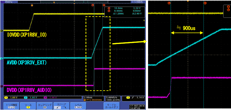
    The upper photo is a power supply sequence of the trial product. Each power supply starts up according to specifications. However, the power good timing of AVDD and DVDD is reversed by slew rate of 3.3 V power. Although AVDD and DVDD order turns over, the customer thinks there is no problem about the power supply sequencing because analog circuits and digital circuits are separated on their trial product board.
    Please tell us your opinion.

    Best regards,
    Akio Ito

  • Luis-san,

    Few months have passed, but let me ask an additional question.

    The upper photo is a power supply sequence of the trial product. Each power supply starts up according to specifications. However, the power good timing of AVDD and DVDD is reversed by slew rate of 3.3 V power. Although AVDD and DVDD order turns over, the customer thinks there is no problem about the power supply sequencing because analog circuits and digital circuits are separated on their trial product board.
    Please tell us your opinion.

    Best regards,
    Akio Ito

  • Ito-san,

    There shouldn't be problem on the board since the analog and digital activity are separated as you mentioned. If power supply sequencing cannot be implemented, customer needs to ensure that analog and digital circuits and ground planes are separated on their trial product board. This will reduce noise from digital to analog side.

    Best regards,
    Luis Fernando Rodríguez S.