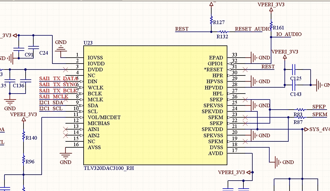
Hi Team,
When use tlv320dac3100 play 48KHz 16bit stereo, we can see correct waveform in pin5 pin6 pin7 pin8, but nothing output in pin23 pin26 pin27 pin30. We can correctly see pin8 MCLK 12288000Hz, pin7 BCLK 1536000Hz, pin6 WCLK 48000Hz as expected. The configuration and schematic as attached.
tlv320DAC3100 Configuration1.txt
# Key: w 18 XX YY ==> write to I2C address 0x18, to register 0xXX, data 0xYY
# # ==> comment delimiter
#
# The following list gives an example sequence of items that must be executed in the time
# between powering the # device up and reading data from the device. Note that there are
# other valid sequences depending on which features are used.
# 1. Define starting point:
# (a) Power up applicable external hardware power supplies
# (b) Set register page to 0
#
w 18 00 00
#
# (c) Initiate SW reset (PLL is powered off as part of reset)
#
w 18 01 01
#
# 2. Program clock settings
# (a) Program PLL clock dividers P, J, D, R (if PLL is used)
#
# PLL_clkin = MCLK,codec_clkin = PLL_CLK
w 18 04 03
# J = 7
w 18 06 07
# D = 0000, D(13:8) = 0, D(7:0) = 0
w 18 07 00 00
#
# (b) Power up PLL (if PLL is used)
# PLL Power up, P = 1, R = 1
#
w 18 05 91
#
# (c) Program and power up NDAC
#
# NDAC is powered up and set to 7
w 18 0B 87
#
# (d) Program and power up MDAC
#
# MDAC is powered up and set to 2
w 18 0C 82
#
# (e) Program OSR value
#
# DOSR = 128, DOSR(9:8) = 0, DOSR(7:0) = 128
w 18 0D 00 80
#
# (f) Program I2S word length if required (16, 20, 24, 32 bits)
# and master mode (BCLK and WCLK are outputs)
#
# mode is i2s, wordlength is 16, slave mode
w 18 1B 00
# (g) Program the processing block to be used
#
# Select Processing Block PRB_P11
w 18 3C 0B
w 18 00 08
w 18 01 04
w 18 00 00
#
# (h) Miscellaneous page 0 controls
#
# DAC => volume control thru pin disable
w 18 74 00
# 3. Program analog blocks
#
# (a) Set register page to 1
#
w 18 00 01
#
# (b) Program common-mode voltage (defalut = 1.35 V)
#
w 18 1F 04
#
# (c) Program headphone-specific depop settings (in case headphone driver is used)
#
# De-pop, Power on = 800 ms, Step time = 4 ms
w 18 21 4E
#
# (d) Program routing of DAC output to the output amplifier (headphone/lineout or speaker)
#
# LDAC routed to HPL out, RDAC routed to HPR out
w 18 23 44
#
# (e) Unmute and set gain of output driver
#
# Unmute HPL, set gain = 0 db
w 18 28 06
# Unmute HPR, set gain = 0 dB
w 18 29 06
# Unmute Class-D, set gain = 18 dB
w 18 2A 1C
#
# (f) Power up output drivers
#
# HPL and HPR powered up
w 18 1F C2
# Power-up Class-D driver
w 18 20 86
# Enable HPL output analog volume, set = -9 dB
w 18 24 92
# Enable HPR output analog volume, set = -9 dB
w 18 25 92
# Enable Class-D output analog volume, set = -9 dB
w 18 26 92
#
# 4. Apply waiting time determined by the de-pop settings and the soft-stepping settings
# of the driver gain or poll page 1 / register 63
#
# 5. Power up DAC
# (a) Set register page to 0
#
w 18 00 00
#
# (b) Power up DAC channels and set digital gain
#
# Powerup DAC left and right channels (soft step enabled)
w 18 3F D4
#
# DAC Left gain = -22 dB
w 18 41 D4
# DAC Right gain = -22 dB
w 18 42 D4
#
# (c) Unmute digital volume control
#
# Unmute DAC left and right channels

w 18 40 00
Could you help to check if any problem in the configuration and schematic?
And any other suggestion for this issue?


