This thread has been locked.

If you have a related question, please click the "Ask a related question" button in the top right corner. The newly created question will be automatically linked to this question.

Seeking advice to digitize 256+ outputs on .5mm- pitch at 40MSPS+ with 14bit+ SNR on Imager Chips.

Other Parts Discussed in Thread: ADC34J43, ADC3443, ADS5294

Hello,


I'm serving as the packaging engineer for a company called ImagerLabs that has some great high-speed imager, low-noise imager chips which have been causing our customers to struggle with the off-the-shelf (14 bit, >40MSPS) multi-input ADCs as they try to design their cameras to fully exploit our imagers.  The imager isn't the main noise source!

Any advice you could supply would be greatly appreciated, especially if a solution already exists.

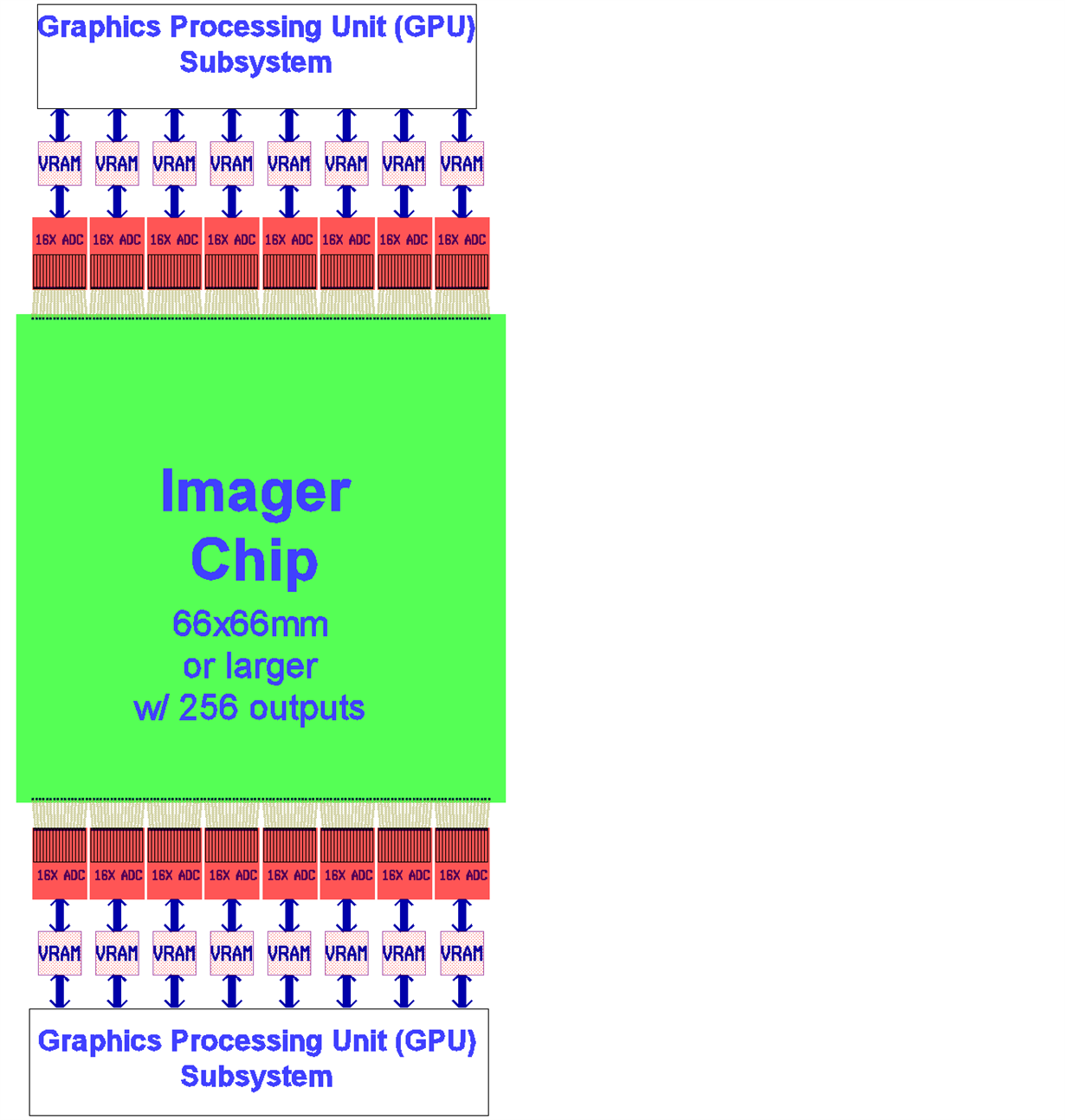
Some of the troubles stem from the electrical distances involved when trying to connect to packaged off-the-shelf ADCs so I'm very interested in a multi-ADC chip designed to be directly wirebonded die-to-die as described below and depicted in the image at the bottom (although I'm certainly open to any better architectures you could suggest).  Note the sets of 16 "gold" wires shown between each 16 channel ADC chip shown in red and the big green imager chip.  Exactly how the data is handled on the other side of the ADCs is wide open to suggestions.

Our imager chips usually have 2 opposite edges dominated with analog output pads, each needing an ADC.  (We typically take advantage of gaps between these outputs by adding supplementary power supply pads, but these need not be of concern to the multi-ADC chip design.)  We would take advantage of whatever ADC input pad density is available from a chip form suitable for direct die-to-die wirebonding where all the inputs are located along one edge. Currently, we have chips with 64 outputs on pitches of less than 0.5mm, and we could go much denser.  Furthermore, our chips can be very large (we're already producing 61mm long runs of outputs; 2 runs per chip though not as dense as we'd like) so it would be quite advantageous if the opposite edge of each multi-ADC chip could host all the I/O needed for it to directly write to a dual ported memory so long rows of these ADC chips (and their companion memory chips) could be abutted into long strips along the edges of our imagers.  I imagine the other port of each dual ported memory (e.g. Video RAM) to be connected to a mainstream graphics processor (GPU or DSP).  Active cooling will be available since our imager chips benefit from that anyway.

At a minimum, 14 actual bits of resolution are needed at speeds of at least 40 MSPS, (preferably 2 to 4 times faster).  The tighter the pitch, the better.  Differential signals are also welcome.  On-chip ADCs from CMOS foundries don't seem to be close to good enough, especially from process lines that make good imager chips.  The ImagerLabs chips already on the market are demonstrating that high performance imaging is already significantly limited just by the available ADC architectures so we would like to tailor future designs to match next generation high-density, high-speed, high-SNR multi-ADC architectures.  The image below depicts just one possible system layout.

This proposed architecture might be very useful to enough other scientific customers/applications that it may be quite possible to obtain government funding so I encourage you to think BIG.  

For one nice example of why higher speed, higher dynamic range. lower noise imagers are still needed to understand our world, I invite you to view the episode of NOVA at:

www.pbs.org/.../edge-of-space.html

If you only have a few minutes, just skip to minute 31.


Thank you for your time,
Mike Fitzsimmons
ImagerLabs, Inc.

  • Into the silence of the past week I'd like to ask about a different way to solve the basic problem:

    Would it be possible to construct hybrid circuit modules, each with a single fiber-optic output that carries the data streams from a large number (64+) of internal high speed, high resolution ADCs?

    This would allow much more flexibility for locating the GPU subsystem.

    The analog inputs should still be arranged along one edge and if there can't be at least 64 inputs (preferably at least 128 inputs), then it would really help if the modules could be abutted like the 16-channel ADC chips shown in the diagram (red).  It would still be nice to have direct wirebondability to these hybrid modules (from the imager chip) and I suspect there are many ways to simultaneously support a row of wirebondable pads in parallel with one of the mainstream surface mount interconnect styles (to better support more traditional uses/users).

    Fiber optic light leaks could be disastrous for an imager chip, so the telecom industry's popular ~1.5um light choice might be fairly safe since it has such low absorption in silicon.  Other supporting technologies from the telecom industry could be leveraged at both ends of the fiber.

    Please let me know of any existing solutions to the basic problem of digitizing high density sets of analog signals, but since it's looking like there's nothing out there, we're also interested in finding partners to help bring a solution to market.  Our imagers are probably not the only products limited by the packing density of high performance ADCs.  Do you know of any other products (or "big science" projects) that would benefit from high density ADCs?


    Thank you again,
    Mike Fitzsimmons
    ImagerLabs, Inc.

  • Mike,


    Sorry it took so long to get any action on this post, but I've moved this into the High Speed Converters Forum. I generally handle low-speed ADCs, so I can't really help on this post, but based on the desired data rate, I think this is the only forum that has the expertise to help on it. You mentioned 40MSPS, but if you're really aiming for double that speed, I think this is the place.


    Joseph Wu
  • Thank you Joseph,

    80MSPS would be very helpful and we would definitely take full advantage of that sample rate.  High speed, low noise, high dynamic range imagers now seem limited by the availability of high density ADCs.  We can probably match our imagers to the best that's out there.

    If industry won't or can't provide them on their own (as seems the case), then we'd like to seek an SBIR and/or other government program to help develop a solution.  Can anyone in this forum suggest other possible end users/applications that might also utilize high density, high speed, high SNR ADCs?  Of course, it's most critical for us to find a partner with the ability to design and fab the ADCs so suggestions would be most welcome for that.  Should I maintain any further hope that Texas Instruments might partner with us on such a project?  I have no other contacts within TI. 

    Thank you,

    Mike Fitzsimmons

    ImagerLabs, Inc.

  • Hi Mike,

    Without reading into too much of the details, have you taken a look at the ADC34J43? Quad channel 14-bit in a small 7x7mm package. Very low power, so thermal design shouldn't be an issue with such high density. The JESD204B output interface is made for high density systems, requiring only two serdes lanes @ 3.2 Gbps for the entire device. The ADC3k family has high SNR and SFDR performance and includes an optional chopper circuit to move 1/f noise out of band which can then be removed through digital filtering. The chopper functionality is only available on the serialized LVDS versions.

    Note there is also a serialized LVDS version called ADC3443 in a slightly larger package.

    Take a look at these two ADCs as a starting point. I think they will be the best options for this application.

    Regards,
    Matt Guibord

  • Hi Mike,

    Another thought, take a look at the ADS5294. It's an 8-channel, 14-bit, 80-Msps ADC with very good SNR and SFDR performance.

    Regards,
    Matt Guibord
  • Thanks Matt,


    The camera makers have already been using very similar octal format ADCs and the large channel density mismatch is what prompted my initial post.

    I would like to find or help create MUCH higher density ADCs not just to support our existing imagers, but future imagers which might very well be limited ONLY by the available ADCs. 


    Thank you for your time,
    Mike Fitzsimmons
    ImagerLabs, Inc.

  • Hi Mike,

    I think you'll need to get in touch with our medical team which typically makes the higher density ADCs. I'll point them to this post.

    Regards,
    Matt Guibord
  • Hi Mike,

    Our group has  developed a 16-channel simultaneous sampling ADC that supports both LVDS or JESD output interfaces.  The device can also be operated in a 32 analog channel configuration but the sampling is not simultaneous as time multiplexing is used.  This device will release to market in June.  If you are interested we can start a dialog offline.  Please email me at ads52j90-support@list.ti.com. 

    Look forward to hearing from you.

    Christian Yots