This thread has been locked.

If you have a related question, please click the "Ask a related question" button in the top right corner. The newly created question will be automatically linked to this question.

DAC8871: Current draw on VREFH-F

Part Number: DAC8871
Other Parts Discussed in Thread: OPA2277, OPA277, INA105, , OPA227, REF102

What is the current draw on the VREFH-F  with a single 10V Ref  when switching at Max Speed and Max code change (full range + to full range -) ?

We are using the OP AMP circuit from the datasheet (OPA2277 without the resistor/capacitor network) but it does not seem to be capable of sourcing the required current.

The current we measure is much higher than the datasheet's Figure 28.

  • Steven,

    Figures 27 and 28 along with the Ref High and Ref Low typical specifications on Page 3 are the best figures we have to refer to for this behavior on hand.

    Can you provide your schematic for this design for verification / review?
  • We also have an Evaluation Board for the part that we are setting up to see if we can duplicate the problem
  • Hi Steven,

    Maybe one more simple set of questions before we go through too many other ideas. How is the output current of the OPA277 being measured in this case? I suppose the OPA277 output drooping was the first indicator that brought you to debug this? What is being done with channel A of U162? When the excessive current is observed what is the loading on the DAC VOUT pin?
  • Just saw your last post

    In the meantime we have the TI Eval board for this in-house and have duplicated the problem.  I will assume that you have a copy of the eval board schematic.

    • We are running the part with an output max change every 1usec. (Measured at J1-6)
    • With the board setup to give the DAC a + and - reference from the on board reference and buffers U5D and U5C
      • If I monitor W7 with a scope I see large negative going spikes every time the data switches and a slow increasing droop in the +10 VDC ref level
      • I see the same at TP1
    • If I change the - Ref to GND by removing W1 and shorting TP2 to AGND the spikes at W7 remain but the droop goes away

    If I go back to the original + and - ref setup and run the DAC 50 times slower the problems goes away and the Vref is solid.

    Our assumption is the part is drawing high current on the reference at  High Speed.  On the original board we measured the voltage across a 2.2 ohm resistor and Vref+ from a external power supply.  The problem went away but we say a current spike that look around 500mA (not sure how accurate that was)

    So this seems to have something to do with the speed we run the DAC at.

  • How is the output current of the OPA277 being measured in this case? 2.2 Ohm resistor, 2 channel scope across it, and then math on the scope.
    I suppose the OPA277 output drooping was the first indicator that brought you to debug this? Yes and very noisy
    What is being done with channel A of U162? Normally U162A gives us a - ref to the part, but we have better results if we remove it and GND the low ref on the DAC
    When the excessive current is observed what is the loading on the DAC VOUT pin? Just a scope probe
  • Hi Steven,

    Thank you for the additional information.

    Would it be possible for you to share the oscilloscope captures of the current spike?

    In the mean time I will likely need to spend some time with a Design Engineer to get more insight on the internal implementation as I cannot readily explain something on the order of 500mA myself. I do not have an EVM board on hand but we can order one as well to replicate things in our lab.
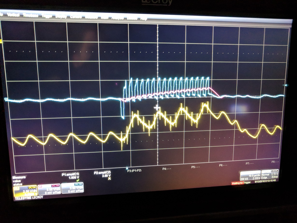
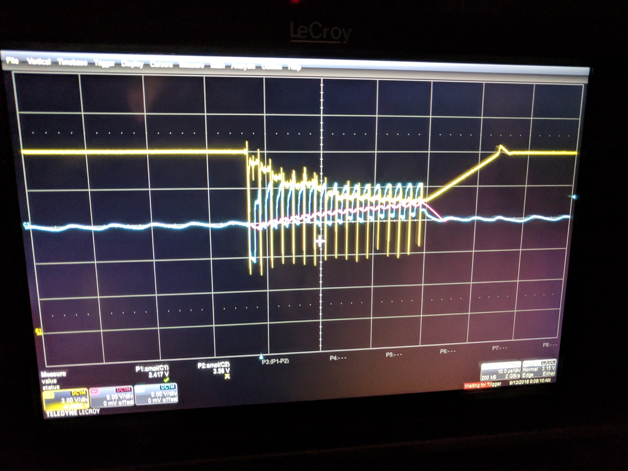
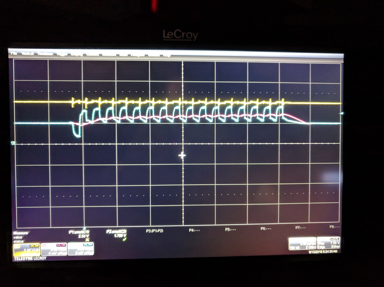
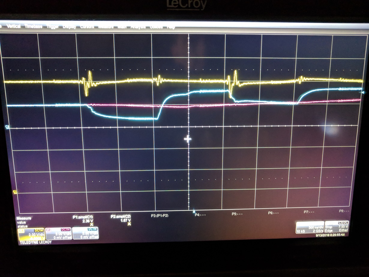
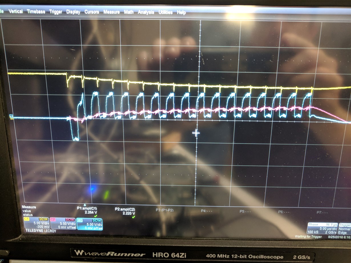
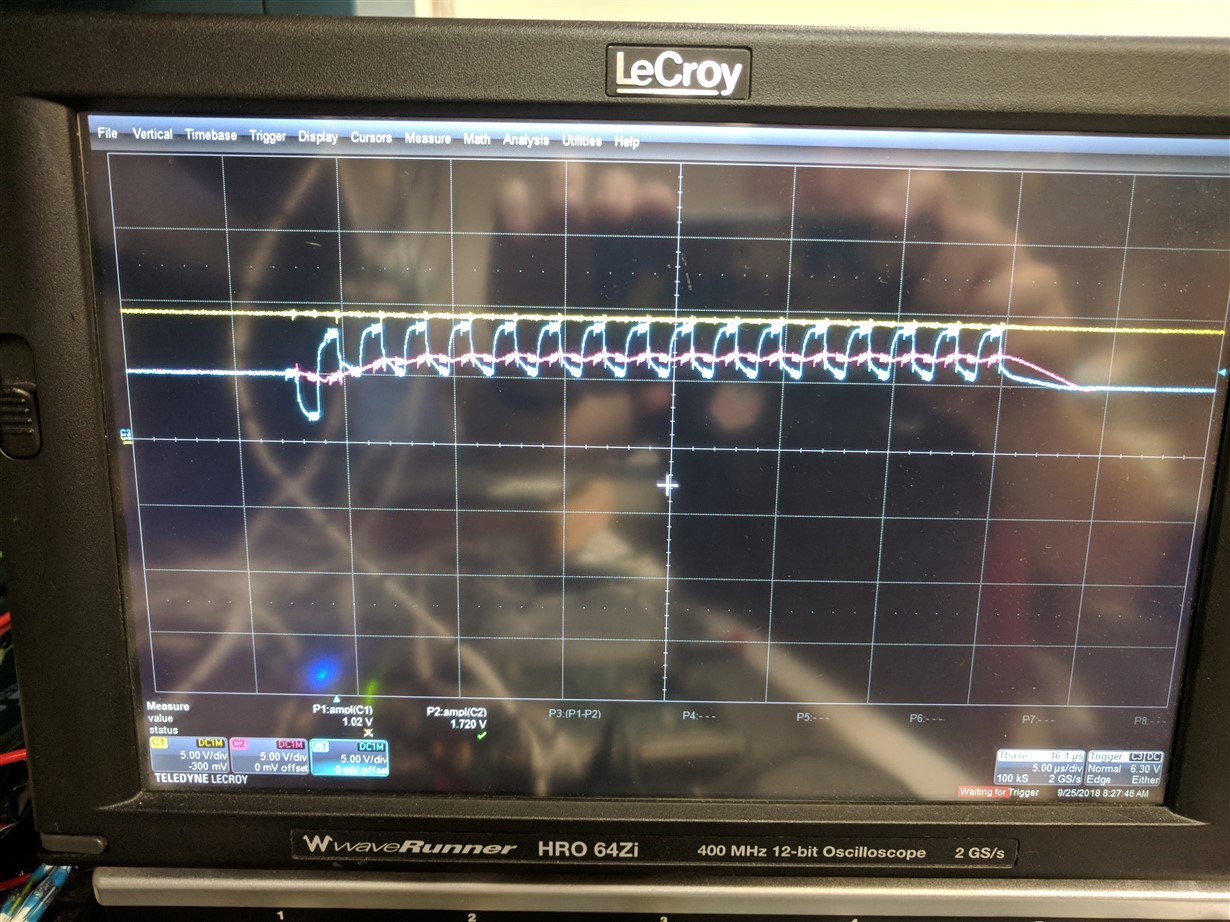
  • The following pictures are all taken from the EVAL board, running ay 1usec switch rate on the output of the DAC, max switch codes.

    Blue is Vout of the DAC measured at J1-6

    Pink is J1-2, the buffered output...We have no idea why the frequency performance is filtered since C1 is not installed

    Yellow is always a reference

    The first picture is with a VREF-P and a VREF-N.   The Yellow line is the negative reference (measured at W1)  for this picture and 2v/div.  The ringing might be a grounding issue on our end, but the droop is not.  We saw the same thing on our custom board

  • This picture is the same setup as above, but the yellow line is the VrefP  monitored at W7 on the eval board, 2V/div on the Yellow line

  • In this picture and the following we have grounded the VrefN.

    The Yellow line is +vrefP measured at  W7, 5V/div...The droop is gone but the noise spike at switching are there.

  • This final picture is a zoom in of the previous to better show the VrefP (W7) voltage spike (2V/div)

  • We cannot directly hook to the VRef pin on the eval board to get you a capture of the current spike. We can do that on our board, but are not currently set up to do it.

    One odd thin we are having a hard time understating is that whatever is happening is flowing back through the U5C and U5D buffers to impact the reference.
  • Steven,

    I also am having a hard time understanding how the nodes at W7 and W1 would be impacted by loading conditions at the outputs of U5D and U5C. Is the INA105 installed on your EVM board?
  • Steven,

    Also, can you comment on the overall current provided to the EVM board from your bench supplies to the board? I'm just trying to dig a bit deeper into what could be creating the impact in these earlier nodes in the signal chain. Is the power supply drooping at all?

    Are all of these results in-line with what you're seeing on your board? Similar or identical?
  • I'm working with Steven on this problem.

    INA105 is installed on our EVM board.
  • On the original board (not the EVM board), we've set the bench supply with a current limit on the +10V of 1A, during which it never hit that limit. It did not droop at all during those tests, and during those tests, the DAC8871 behaved exactly as described in the datasheet. In this test, we were able to inject the bench supply +10V into the REFH rail directly w/o going through any additional buffers/

    On the EVM board, there is no way to inject the same supply directly into the DAC8871 (w/o the OPA4227UA), short of cutting traces and lifting pins on the EVM board. So, this test hasn't yet been run on the EVM board.
  • Have you been able to duplicate the problem on your end?

  • Steven,

    I have been and am out of office on business travel an unable to test this as the EVM board did not arrive prior to my departure.

    Meanwhile, a member of my team, Uttama Sahu, also has an EVM on the way and will work to reproduce this in his lab.

    Also, what I meant earlier with my question concerning your board was whether you were observing this droop on the reference buffer outputs, the reference source output when it was the on-board reference, or both? On the EVM seeing these effects at the jumpers before the buffers is very surprising to me if the culprit is really supposed to be current draw from the output of the buffers.

    Are RP1 and R14 also installed on your EVM? What was the setting for W1 in your EVM-based tests?
  • We are observing the droop at W7 (directly following the reference source output), at TP1/W3 (following the OPA4227UA at U5A), and also at U5-14 (following the second OPA4227UA, which directly feeds the DAC8871's Vrefh-f input).

    RP1, R14 are both installed.

    W1 has 1 and 2 connected.

  • Hi Dave,

    Sorry, but to clarify once more, what I am asking is if you see the reference source disturbed on the board which you designed (not the EVM, what was previously referred to as the "custom board") or if the observation on your design was at the buffer outputs. Just trying to determine if the two observations are equivalent or not. I suspect in your design the observation was truly at the output of the buffers, and not from the reference source.

    Concerning the EVM it seems like our contract manufacturer may have made some mistakes building the board as the schematic note indicates that U5B and RP1 should only be installed as a replacement circuit if INA105 is not available. Fundamentally I don't follow the note as one could not simply choose to not install U5B since this is a quad op-amp and the other channels are required. Perhaps you can remove R14 to effectively remove U5B from the circuit, but still leaving RP1 installed such that the op-amp can still operate closed-loop and not consume excessive current and potentially impact the other channels. Alternatively you could remove the INA105 but removing the resistor should be easier.

    If both circuits are populated they will be competing for regulating the load at the input to W1. Ideally their outputs would be very similar but error parameters etc. will not make that the case of course. I'm concerned that this is potentially a path which is causing an impact at W7 on the EVM. This could impact both the measurements at W7 and at W1.

    Also, I believe the root cause of the ringing you've observed on the EVM is probably C13. Neither INA105 nor OPA227 are going to be happy directly driving that load with no series resistance from a stability perspective. So I would suggest removing C13 from the EVM as well.

    I am not happy with this EVM design to say the least, but it had not really been brought to my attention to this point. I apologize for these issues with this legacy EVM design.

    At least with the modifications proposed, I think we can have a more 1:1 setup on the EVM to your custom board and be able to really use the EVM to check whether this is a reference input current issue and drive strength issue for the buffers, or if indeed something else was happening on the EVM board and perhaps something else as well then on your custom board.
  • I re-ran the test on the custom (our) board, and the voltage disturbance is only on the output of the buffer (the OPA2277A) and not the voltage reference (AD01).

    I am working on getting the R14 and C13 components removed and should have those test results tomorrow.

  • On the EVM board with R14 and C13 removed, in the standard (default) jumper configuration, the sharp voltage disturbances measured at W7 are reduced, but not eliminated.  See attached

  • Same setup as previous, with W1 removed and vrefl circuit grounded at TP2.  See attached

  • Hi Dave,

    Thanks. This is encouraging improvement but I'm still vexed by how the REF102 is being impacted. I just returned from travel today and Uttam received a board this evening in India. He will be testing this on the EVM himself in our labs tomorrow and provide his inputs. If it's some EVM level nuance he should be able to track it down and get us to a point where we can finally make a comparison on the reference drive capability alone without other factors.

    The VSS rail (-15V or so) is applied on your EVM?
  • Yes, the VSS rail is set to -15V on the EVM, supplied by an external triple DC bench power supply.

  • Dave,

    We've looked at this internally now for a bit on the EVM and I cannot find any reason why the reference output itself is showing this transient behavior other than perhaps some layout concern.

    In any case, as you've observed with an external reference source it does appear that the EVM circuit does not appropriately drive the reference inputs and the suggested circuit in the datasheet, which has no values assigned to the discrete components, is not very helpful nor implemented on the EVM - furthermore I have concerns about whether that design would successfully drive the inputs as well without creating a stability issue for the buffers.

    My team and I are going to build a new board to evaluate this and suggest a better circuit for driving the reference inputs. In my experience topics like this must be evaluated in HW as switching input parasitics are not perfectly modeled in simulation. We'll build that board, come up with a better proposal, and come back to this thread with that update. Should you want a copy of the hardware which fixes this in the end, we can ship that to you.

    Second - we will update the EVM hardware and user's guide, the datasheet, and publish a reference design for appropriately driving these DAC reference input topologies.

    I apologies for the frustration and the delays on this - obviously there are a number of things that have failed on this which unfortunately came before me, but we're going to get it cleaned up.