This thread has been locked.

If you have a related question, please click the "Ask a related question" button in the top right corner. The newly created question will be automatically linked to this question.

using DAC3162EVM evaluation board

Other Parts Discussed in Thread: DAC3162EVM, FMC-ADC-ADAPTER, DAC3162, CDCP1803

Hello, we are trying to create a sine and cosine wave from an fpga evaluation board ( virtex6 ML605 evluation board). We bought the DAC6132EVM and the FMC adaptor for it because the virtex6 has the FMC connection. The problem we have is that the DAC has to be configured and apparently it comes configured for CDMA modulation.

The wave we are trying to create does not have to be modulated and therefore we do not need the modulator to be activated. We followed the guide dac3162evm.pdf (http://elcodis.com/parts/3499641/DAC3162EVM_dt633792.html). It explains how to test the converter using a TI function generator board. We used the FPGA to generate the information and send it to the FMC connector >>adapter>> DAC. We do not need WCDMA modulation so reading the same guide we found it talks about setting the board to only DAC conversion. Now the problem is the guide says to remove resistors R109, R110, R111, R112. They are micronized resistors and we are not too comfortable removing them nor sure if this is correct for what we need to do. 

If some one could clarify if we need to actually remove the resistors or if there is a different way of setting up the converter it would be greatly appreciated. We have read the files in http://www.ti.com/tool/dac3162evm?DCMP=analog_signalchain_mr&HQS=dac3162evm-pr and have not been able to understand it completely or find a guide which explains what is being done. 

Thank you for any help. 

Extra notes: its actually "DAC3162EVM evaluation module", and we are using look-up tables in the code and sending the information to the DAC.

  • Hello Manuel,

    I'm transferring your post to our converter group.  They should be able to help.

    Thanks

  • Hi Manuel,

    Take a look at the design package on the EVM website (http://www.ti.com/litv/zip/slar057). There is a schematic in there that should be helpful.

    I'm not sure what you mean by "the DAC is setup for CDMA modulation". If you're referring to the IQ modulator on the board, the default board should not use it. In order to use the transformer outputs (IOUTA2, IOUTB2) all the resistors you mentioned SHOULD be installed. Removing these resistors (plus installing R191,195,207,211) will actually enable the modulator. Take a look at the schematic mentioned above to make sure you understand how these resistors are configured.

    The User's Guide makes it look like the modulator is enabled by default. You'll need to look at the board you have to figure out which configuration it is in. If R109,R110,R111, and R112 are installed, then the transformer output is enabled. If they aren't installed, the modulator is enabled. You would need to switch these resistors to change the configuration.

    Regards,
    Matt Guibord

  • I'm sorry maybe i wrote too much and didn't make much sense. We are trying to figure out how to transfer the information through the FMC connection to the adaptor&ADC. We assumed all we needed was to feed the information bits and a clock. We saw the schematic you pointed out and also file slar101 which has a shcematic for the FMC and DAC pin connection.

    We need to find out how the information is fed into the FMC-ADC, we assumed that we need only to provide the bits of information in the fmc adaptor pins which are IO_0P/N-I0_11P/N, we assumed we needed to feed a clock to the adapter and used pins FCLKP, FCLKPN. We are unsure if we need to use DCLKP, DCLKN, SDATA, SCLK. We used FMC-ADC-ADAPTER_C_SCH.PDF and DAC31x2EVM-B_SCH.PDF to try and figure out which pins on the DAC Module Board (J2 ) connect to the DAC chip inputs and to figure out which pins on the FMC connect to the needed pins in J2 on the DAC Module Board.

    We are a bit lost, as we are somewhat new to this, and the documentation does not have many examples or clear information on how to implement different uses of the DAC. Another concern has been if we just give the DAC a 'regular' clock from the FPGA or a DDR clock as pointed in the datasheet of the DAC chip (DAC3162 data sheet.pdf). 

    Thank you.

  • Manuel,

    First off, you're looking at the wrong connector. You need to look at the FMC_DAC_ADAPTER, not the ADC adapter. This may be the source of your confusion.

    http://www.ti.com/tool/fmc-dac-adapter

    Note that the DAC gets its clock from the CDCP1803 on the EVM board. You'll need to supply a clock to the CDCP1803 through the clock input SMA on the DAC31x2 board. The CDCP1803 also supplies a divide by 4 clock (clock in to CDCP / 4) to the FPGA through the FMC adapter. This would be the signal "FPGA_CLK" on the FMC adapter. Note that there is no clock coming back from the FPGA to the DAC because the output sampling clock and the data clock are the same signal (DACCLK) for the DAC31x2. What this means is that you'll need to guarantee correct timing of the data to the DAC with respect to the clock signal going to the DAC from the CDCP adapter. This is in contrast to most of our DACs that have both a DAC output clock and a data clock, where the data timing is referenced to the data clock coming from the FPGA and the DAC clock is simply used to clock out the analog signal. The DAC31x2 DACCLK signal provides both functions.

    Take a look at the correct adapter and see if this makes more sense to you.

    Regards,
    Matt Guibord

  • Thank you very much. We were actually looking at the wrong revision of the document. Now with this info we are concerned, about a couple things.

    1) We were under the impression the converter could go up to 250MHZ (since sampling max is 500MSPSs) or atleast 70mhz which is seen on the data sheet of the chip dac31x2. Threre are different values on that data sheet, and no datasheet for the whole evaluation board. This is a concern because now we are thinking if the clock fed back from the DAC through the FMC to the FPGA is divided by 4 then that would make it 500MHZ/4 = 125MHZ. Is this the clock frequency at which the chip will sample the data? if so then the maximum of the evm board is probably very low which is not good for us.

    2)Secondly, i am assuming that the clock fedback is for the FPGA board to time the data correctly and have it latched on the rising and falling edges? if so do we have to implement the IDDR or ODDR scheme whcih is seen in other threads? like this one http://e2e.ti.com/support/data_converters/high_speed_data_converters/f/68/t/47555.aspx, this is for an ADC but i imagine its is somewhat similar to what we need to have the data on time for the DAC clock.


    Thank you for your help.

  • Manuel,

    The clock fed back to the FPGA is set to the correct frequency to pull the data out of the onboard memory. We then use a PLL to convert it to the correct sampling frequency. For instance, on the DAC3162, we send DACCLK/4 to the TSW3100. It uses DACCLK/4 to access the onboard memory to pull the pattern out. Then it uses a PLL to create a data clock of DACCLK/1. Note that this implementation is very specific to our TSW3100 and TSW1400 based on how we've decided to implement the source code. We also probably could have used DACCLK/1 into the device and then divide it down internally to access the RAM. I'm not sure why it was decided to do it one way over the other.

    For example:
    Running the DAC3162 at 500 MSPS (500 MHz DACCLK), the FPGA uses 125 MHz to access the RAM, and uses a PLL to output the data at 500 MSPS (clock at 500 MHz, data at 1 GHz because of dual data rate). So the actual sample rate for the DAC is 500 MSPS. This means you should be able to output a signal up to 250 MHz (full first nyquist zone). The DAC itself is will be outputting 500 MSPS from each channel.

    The clock coming back is used for two purposes. The first is to pull the pattern out of the RAM on board, we do this at DACCLK/4. The reason is that the RAM is 64-bits wide and thus we are pulling 4 samples (64-bits) out of RAM for each clock edge (rising and falling) so 128-bits per cycle (8 16-bit samples). We then use the serdes block of the FPGA to convert from a 128-bit wide signal to 16-bit wide samples in DDR format. These samples are output at DACCLK/1 in DDR format so 4 of the 8 samples are output on the rising edge, and the other 4 on the falling edge for a total sample rate of DACCLK/1 (DDR).

    Regards,
    Matt Guibord

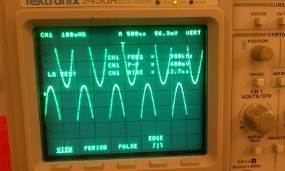
  • Hello again, the information you gave us was very helpful to get us going in the right direction. We also realized that we had used the wrong pins for the data since the pin change from dac>>fmc>>fpga was a little confusing. We believe we finally got the right data pins and possibly the clock synchronized, however we have a problem because we are gettting a wierd sine. The first half has an arch down and the second an arch up, pretty much both with the peak pointing to each other.

    We have attached a picture of the result. We did some reasearch and it might be the signed or unsigned numbers from the DDS in the FPGA. The data we produce from the DDS is coming out signed and we are not sure if the DAC is made to receive signed or unsigned, and/or if it has a jumper setting that might allow either of the two.


    We are working on a solution to unsign the numbers and test the DAC but wanted to get your input to see if we are on the right track as we are a couple weeks from the deadline for the project. Your help is very appreciated and here is the picture of what we obtained when sending signed data to the DAC.

    Thanks.

  • Manuel,

    I agree with you, this does look like a 2's compliment vs. offset binary problem. The DAC3162 needs an offset binary input, it cannot be programmed to accept 2's compliment.

    I believe you can just apply an XOR function on the MSB (XOR the MSB with a constant 1).

    Regards,
    Matt Guibord

  • Hi, your advice has been very useful. It was what you pointed out, the DAC is taking offset binary and we were sending 2's complement  binary. Reading a little more we found out one can change 2's complement to offset binary simply by changing the MSB into the opposite value like you told us. We tried it using a inverter and also an xor gate and both worked. 

    The only problem we have now is that the cleanest wave we can achieve is at about 30MHZ after that the wave starts getting some distortion and can go up to maybe 60MHZ without looking completely different but not good enough in terms of a signal to be transmitted. Reading more on sampling theory i see that every cycle has to have at least 2 samples accoridng to nyquist but that will not give us a good enough wave, we have tried using  5 or 6 samples and that would give Fout of about 100 to 83 MHZ.

    My question now would be in your opinion can the DAC get to these frequencies and produce a decent enough sine wave for transmittal (through coaxial cable). We are unsure completely if we are simply having timing issues with the data or if its only because of the number of samples, and maybe rise & fall time, of the DAC are causing this distortion. 

    We saw in the documentation that from spectrum analysis for the DAC3162 datasheet.pdf that they only test 10MHZ and 70MHZ, however we can't see any samples of any wave produced and we are at a loss if the extra sidebands and noise on the 70MHZ comparison would cause such great distortion.

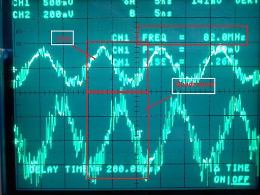
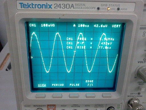
    Below are the first pictures we took; one is at ~4MHZ and the second is at ~ 82MHZ. I will post newer ones later on since there's been some design changes which made it look good up to 30MHZ. Thanks for the help again. 

  • Sorry the ~4mhz picture did not upload. Here it is and the newer one as well:

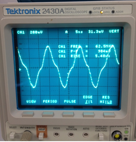
    With some changes to the design picture at ~63 MHZ

  • Manuel,

    The DAC3162 should be able to produce a cleaner sinewave than what you're seeing. Most of my experience with DACs is using a spectrum analyzer to look at the frequency content. This is often much more useful than looking at an oscilloscope. Therefore, it's hard for me to visualize what may be going on here. Do you have a spectrum analyzer available?

    Secondly, make sure the oscilloscope is set to be 50 ohms in and not 1 M ohm in. This could cause reflections.

    Third, are you using the default EVM configuration? Are you looking at the transformer output?

    Lastly, the DAC will have images. As you move your output frequency toward Fs/2, the first image will move from Fs toward Fs/2. If your output frequency is very close to Fs/2, your image will also be very close to Fs/2. This can make a clean spectrum on a spectrum analyzer look like garbage on the oscilloscope. That's why it's important to look at the frequency spectrum, much more information can be pulled from a plot of frequency vs power than time vs. voltage. Keep in mind that images are a perfectly normal part of the DAC and that low pass anti-aliasing filters should be used in a real system to filter out the images, leaving only the clean desired sine wave left.

    As an example, consider the following scenario: Take a DAC running at 100 MSPS with an output frequency of 33 MHz. Sampling theory tells us that this is acceptable because Fout < Fs/2. If you consider the time domain output, you will see 3 samples per cycle. On a scope, this will look like a very distorted signal because there will be fast transitions at each sampling point and then a single voltage held until the next sample. Realistically, our desired 33 MHz is within the signal in all its glory, however it's being "hidden" or distorted by the sampling images at Fs-IF (66 MHz), Fs+IF (133 MHz), 2Fs-IF (166 MHz), and so on. These images give the time domain signal it's square look and fast transitions, but realistically its the zero order hold output of the DAC that creates these images. If we can filter out the images using a low pass anti-aliasing filter we'll be left with our 33 MHz sine wave only.

    Regards,
    Matt Gubord

  • Thanks, again. We are currently looking into the possibility of the filter and were able to get some pictures with a spectrum analyzer i will post them later on so you can see the frequencies and power we are achieving. I have a question however that is very important to us at the moment. Per the spectrum analyzer we are achieivng a -3dbm power and we need to get to 10dmb(as a minimum) for the signal to be able to operate with the signal. We are wondeirng if the EVM board has any power amplifiers, and we are looking as the schematics as we post this. THanks again your help has been extremely helpful to us.

  • Hi Manuel,

    Sorry for the delay. You've probably figured this out by now, but the DAC is not able to achieve 10 dBm output power by itself. Use of a 4:1 transformer can get you closer to 4 dBm, but you'll still need an amplifier to achieve 10 dBm.

    Regards,
    Matt Guibord