This thread has been locked.

If you have a related question, please click the "Ask a related question" button in the top right corner. The newly created question will be automatically linked to this question.

ADC ADS62P48 CLOCK INPUT

Other Parts Discussed in Thread: CDCE62005, ADS62P48, CDCE72010, ADS62P45

Hello,

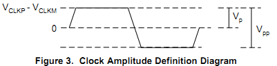
I am using clock synthesizer CDCE62005 to provide clock to ADC ADS62P48. I am attaching a document specifying LVPECL clock output voltage levels of CDCE62005 and LVPECL clock input voltage levels of ADS62P48. Kindly confirm whether this interface will work.

Thanks

Radhika

  • Hi,

    i did not see any attachment.

    The ADS62P48 can accept an LVDS clock, but it must be AC coupled since the clock input to the ADS62P48 must be centered about a 1.5V common mode voltage and an LVPECL driver would likely be centered about a 2.0V common mode voltage.  So the PECL output from the clock chip would have whatever bias resistors the driver would want to see, then AC coupling caps or possibly transformer coupling, and the ADS62P48 clock input would then be able to internally bias the clock swing to the desired input levels that the ADC wants to see.

    The EVM for the ADS62P48 includes a CDCE72010 clock chip on the EVM for the option of using the LVPECL clock outputs from the clock chip.  So for an example of how to use the LVPECL output, that EVM would be a good reference.  The LVPECL output is not the default option as the EVM is delivered, but the User Guide for the EVM describes the soldering needed on the EVM to use the LVPECL clock.  The User Guide and the physical design package that includes the schematics can be found at the product folder on the web for the ADS62P48 EVM at http://www.ti.com/tool/ads62p49evm.  Either revision C or revision D User Guide and physical design package would be acceptable for this purpose - they both have the CDCE72010 clock option and would make a good reference for what you want to do.

    As can be seen in the schematics for that EVM, the PECL clock output has a resistive bias network that the LVPECL driver requires, then there is transformer coupling and series AC coupling caps.  The transformer coupling is optional - your choice.  The default clock option for the EVM is single ended clock input from a signal generator so the transformer was needed for single ended to differential conversion and the transformer was simply kept in place for the LVPECL clock option.  The User Guide suggests that the resulting SNR for the LVPECL clock option would be reduced due to the fact that the LVPECL clock has no filtering to remove phase noise from the various components in the clocking path, and Figure 11 of the User Guide shows a slight loss of SNR compared to the other two clocking options on the EVM.   The default clock option for the EVM assumes an external narrow bandpass filter from the signal generator to remove unwanted phase noise from the sig gen, and the other clocking option on the EVM is using a CMOS output from the clock chip and running that through a crystal filter and transformer coupling.  Comparing those options to the LVPECL option you can see that the EVM has no filtering in place for the LVPECL option and so the SNR is degraded a bit.  You could add your own simple LC bandpass filter on the LVPECL clock lines after the AC coupling if you wished - that is often done.

    Regards,

    Richard P.


  • Hi

    Following is the data given in the ADS62P48 datasheet


    Following is the data given in the CDCE62005 datasheet

    The input and output voltage levels are not compatible. Kindly confirm.

    Regards

    Radhika

  • Hi Radhika,

    The voltage levels are compatible. The CDCE62005 datasheet is listing the amplitude of the swing whereas the ADS62P48 datasheet is listing the peak-to-peak value. Therefore, the CDCE62005 peak-to-peak output voltage is 1.22 to 1.94 Vpp. These are compatible.

    Realistically, any clock that is larger than 0.2 Vpp to will work with the ADS62P48 (as shown on the "sine wave, ac-coupled" line), as long as care is taken to not exceed the absolute maximum conditions of the part.

    Regards,
    Matt Guibord

  • Hi,

    we are planning to use ADS62P48  in place of ADS62P45 in our Digital  Radio project.

     I have some queries  please  clarify:

     1.All digital inputs support 1.8V and 3.3V CMOS logic levels mentioned in the data sheet.But DRVDD supply was 1.8V ,How it supports  for 3.3V?

     2.Can I use 1.8V LVDS logic level to the clock input ? 

     The Evm schematic specifies logic levels of 3.3V  for CLKP, CLKM(2), RESET, SCLK, SDATA, SEN, CTRL1, CTRL2 and CTRL3 is it correct or can I use 1.8V logic levels for above signals?

     Let me know the voltage levels  of Digital inputs i.e: sclk,sdio,sen,reset and clkoutp/clkoutn.

    Reg,

    Uma Mahesh

  • Uma,

    The digital inputs run off the 3.3 V analog supply so that they will be 3.3 V tolerant. They are compatible with 1.8 V CMOS levels as well, as given by the input switching thresholds in the electrical table. Note that SDO (SPI readback) is only 1.8 V, so a level translator would need to be used if interfacing with a 3.3 V processor/FPGA.

    And yes, an LVDS clock can be used. This is listed under the "CLOCK INPUT" section in the electrical table.

    Regards,
    Matt Guibord