This thread has been locked.

If you have a related question, please click the "Ask a related question" button in the top right corner. The newly created question will be automatically linked to this question.

Using ADC12J4000EVM & TSW14J56

Other Parts Discussed in Thread: ADC12J4000EVM, ADS42JB69, DAC38J84, ADC12J4000, DAC38J84EVM, LMK04828

I am using ADC12J4000EVM & TSW14J56.

TSW12J56 has ALTERA FPGA. However, I want to run ADC12J4000EVM with our own Xilinx FPGA board.

Would you please offer the FPGA Referrence Design of TSW14J56, HDL,Firmware...etc?

I try to change the design to Xilinx.


Best Regards,

H Tobe

  • Hi Tobe,

    Can you wait a week or two?  We (TI and Xilinx) are in the process of releasing a solution that would allow you to use a KC705 platform+ADC12J4000EVM with HSDC Pro.  This would effectively allow you to do evaluation using Xilinx IP.

    Xilinx field apps would then be able to support your needs for example projects etc.  Do you have access to a KC705 platform?  I think  this will save you some work if you can get access to a Xilinx-supported solution.

    Ken.

  • Hi Ken-san,

    Thank you for your greate answer.

    I have KC705 and want to receive the Xilinx desgin.

    Would you please tell me the download site after releasing?

    Is Xilinx IP free of charge?

    Best regards,

    H.Tobe

  • You will have to work with your Xilinx Support person to get more info on the IP from Xilinx.  We will only provide a compiled bit file that will be loadded into the KC705.  The project itself is owned by Xilinx.

    We will provide a link once the project is ready for release.

    Ken.

  • Hi,

    Is that mentioned design for the Xilinx KC705 + ADC12J4000EMV already available somewhere ?

    Regards,

    Erik

  • Hi,

    Xilinx released TI HSDC Pro Reference Design in JESD204B Evaluation Lounge.

    I am not sure that it supports AD12J4000 and going to try it.


    Regards,

    H.Tobe

  • Thank's for the update. Did you have a chance to try it out ?

    I looked at the KC705 user guide and according to that, only four GTX transceivers are connected to the FMC HPC connector on the KC705 (one TX transceiver connected to the FMC LPC). So I don't see how the 8 lanes used in the TI HSDC Pro Reference Design will work with the KC705. The KC705.xdc, part of the TI HSDC Pro Reference Design, is using (GTXE2_CHANNEL_X0Y8 - GTXE2_CHANNEL_X0Y11) which are supposedly connected to SMA, SGMII, SFP+ and FMC LPC DP0) on the KC705. Does that design really work on the KC705???

    I couldn't find any documentation on the TSW14J01 that is mentioned in the TI HSDC Pro Reference Design documentation but it might work with that board since it seems to be wired differently.

    I think there is a problem in the reference design documentation.

    I'm missing something here?

    Regards,

    Erik


  • Erik,

    With the release of the TSW14J10 which Xilinx fully supports for the KC705 platform, it was decided that the TSW14J01 would not be officially released, but instead would remain as an internal development EVM.  The documentation will be updated to reflect this in a newer release.

    The TSW14J01 was routed slightly differently with the connection of 8 lanes to the FMC as opposed to the 4 lanes on the Xilinx KC705 FPGA platform.  4 lanes in most cases is adequate, however in cases where 8 lanes is desired another platform will have to be used as the Xilinx KC705 FPGA platform only has 4 lanes routed.  We are working with Xilinx to enable 8 lanes on another Xilinx platform.  This will be available soon.


    Currently the TSW14J10+KC705 has been validated for the DAC38J84 and ADS42JB69 family of EVMs - We will be enabling other JESD204B converters on this platform on a priority need basis.  Can you confirm which device and which mode you need and we will prioritizing this?

    Thanks.

    Ken.

  • Tobe,

    Which mode of ADC12J4000 do you need?  8 lane Bypass mode or some other decimation mode?  We are validating other converters and modes on a customer request basis.  Only the DAC38J84 and ADS42JB69 have been validated as of this release.  However the other converters and JESD204B modes should not pose a problem as the interface is standardized - we just need to validate config files and release them.

    Thanks,

    Ken.

  • Ken,

    Thank you very much for your detailed response. It makes a lot of sense to me. I'm interested in the ADC12J4000EVM+TSW14J10+VC707.  I would like to use a Xilinx VC707 since I have it already in the lab and it allows 8 lane connectivity on the FMC. I would be interested in the 8 lane bypass mode and maybe want to try the decimation filter settings later also.

    I would greatly appreciate if the VC707 would be supported as a platform for the Reference Design.

    Would it be possible to give a timeline or some range maybe? Is it 1-2 weeks or do I have to expect months?

    Regards,

    Erik


  • Erik,

    As we don't control the development of this IP (Xilinx owns this firmware development) it is difficult to commit to a date.  However both Xilinx and TI are aware of the need and we will do what we can to see if we can have a version released in 2-3 weeks time that supports 8 lanes on the VC707 platform.

    Ken

  • Hi Ken-san,

    I want to use ADC14J4000 as 4 lane Bypass mode at 1.96608GSPS.

    This speed is enough to transfer data by using 4 lanes.

    Does ADC14J4000 support 4 lane mode?

    Should I modify some registers by Law Level View on EVM GUI?


    I didn't find any register map in ADC12J4000 datasheet.

    Let me know which register I should modify in ADC12J4000.


    Regards,

    Tobe

  • Hi Tobe

    The ADC12J4000 always has all 8 lanes active when operating in the DDC Bypass mode. Operating with only 4 lanes would require the output clock rate to be muliplied by another factor of 2 and that capability is not included in this device.

    If your capture solution is limited to 4 lanes you have a few alternative modes that could be used:

    1. Use the ADC in DDC Bypass Mode with a clock rate 2x the sample rate you need (3.93216 GSPS), but only capture the data from 4 of the 8 active output lanes. Essentially you only be capturing every second data sample. This will effectively decimate by 2 and give the desired sample rate. The disadvantage is running the ADC faster than is needed, and the resulting higher power consumption.
    2. Use the ADC at 3.93216GSPS in Decimate by 4 mode. This will give a complex output sample rate of 983.04 MSPS and an alias free bandwidth of 786.432 MHz (-393.216MHz to +393.216MHz).

    Hopefully one of these 2 alternatives can work in your situation.

    Best regards,

    Jim B

  • Hi Jim-san,

    Thank you for information.

    I try to do Case2 first, and then Case1.

    TSW14J10EVM(Interposer) just arrived yesterday.

    Can HSDC SW get a data when I setup case2?


    Regards,

    Tobe

  • Hi Jim-san,


    HSDC Pro SW is not running by using KC705 and TSW14J10.

    The SW try to find a file of \14J10 Details\Device and File Info.ini.

    However, there is no \14J10 Details\ folder in the path.

    \14J10KC705 Details\ folder exists in the path.

    HSDC Pro GUI version is v2.70. Dll is 0.0.  No patch.

    Let me know what should I do.


    Regards,

    Tobe

  • Tobe,

    If there is a 14J10 Details folder, please remove it. and re-run HSDC Pro.  The 14J10 Details folder was left over from a previous installation of HSDC Pro.  You can also uninstall HSDC Pro from Control Panel, then manually delete the High Speed Data Converter Pro folder and re-install HSDC Pro - this will be a fresh install of 2.7 and should have no problems.

    The error is happening because HSDC Pro is not detecting a valid KC705 through the JTAG connection (please connect the JTAG cable from TSW14J10 to KC705) and by default the board TSW14J10 is the default EVM and it tries to scan the file in the TSW14J10 Details folder.  Normally if this folder does not exist it would ignore and indicate that there is no board connected - we have fixed this in an internal release so that if it does not find a valid JTAG ID for the attached FPGA platform it will report no board connected.  This will no longer be an issue in a future release.

    Once you have the JTAG cable installed and the 14J10 Details directory removed then HSDC Pro should start normally and detect the KC705.

    Our apps team willl work with you on getting the ADC12J4000 working once you have this up and running.

    Ken

  • Hi Ken-san,


    Thank you for your information.

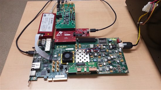
    I connect Xilinx USB cable to KC705 as you see the following picture.

    After write a bit to FPGA, I remove Xilinx USB Cable and connect KC705 and TSW14J10 by flat cable.

    HSDC Pro is running and showing  "Interface Type = TSW14J10_KC705".


    I have two questions.

    1) Xilinx SDK

    I want to modify an example program called tsw.c by using Xilinx SDK.

    In this case, Xilinx USB Cable must be connected to KC705.

    Is it possible to run HSDC Pro and Xlinx SDK?

    2) Select ADC

    HSDC Pro for KC705 supports only ADS42JB69 now.

    Let me know how to get ADC12J4000 data via KC705 by using HSDC Pro.

    Do you support such combination?


  • Hi Tobe,

    The combination you have TSW14J10+KC705 and ADC12J4000 is something that will be supported in a week or 2.  This platform is fairly new and we are adding more modes to it for our customers.  Currently as you can see it only supports ADS42JB69 and DAC38J84 EVMs.  If you need to do evaluation of the ADC12J4000 you can always start with TSW14J56 (Altera based).

    One note, the KC705 only has 4 serdes lanes routed on the HPC FMC connector - this means that the ADC12J4000 can only run in decimate mode, and not in true bypass mode at the full sample rate of the ADC12J4000.  To explore the 8 lane bypass mode of the ADC12J4000 you will need to possibly use another platform such as the VC707 which has all 8 lanes routed on the FMC connector - HSDC Pro and TSW14J10 adapter will support this platform in the near term - the firmware is being verified at this time.

    The apps engineer supporting the ADC12J4000 will comment on this thread once he is has completed verification of the ADC12J4000+KC705/VC707.

    Thank you for your patience.

    Ken

  • Hi Ken,

    I see VC707 has two HPC FMC connectors, would it be able to support two ADC12J4000EVM both in bypass mode?

    Thank you,

    Cristian

  • Cristian,

    Yes it can if both HPC ports are routed with the appropriate SERDES connections.  However it is not a standard mode that we support on the TSW14J10+VC707 and would be something you would have to do in terms of implementing 2 JESD cores and then combining them on the VC707 firmware - your custom firmware.  Also if you want synchronization that is something that will have to be worked out as well to ensure the clocks/sysrefs are the same for both ADC12J4000 from a synchronization stand point.

    We are working on these issues and is something we can help with once we verify it all works as expected.  Sorry as I do not have any more news than that for now.

    Ken.

  • Hi Ken-san,

    Thak you for your information.

    I am going to have VC707 and looking forward to getting the comment.


    Best Regards,

    Tobe

  • Hi -

    Any news on the release of the support of the ADC12J4000EVM directly on the vc707 platform? Will there be a reference design available?

    Regards,

    Marc

  • Hi Marc-san,

    Xilinx has no plan to release VC707 Ref. Design of ADC12J4000.

    Please access to the following Xilinx web site. You see the answer.

    Xilinx User Community Forum >...> Xilinx Board and Kit > JESD204B Ref. Design for VC707 and ADC12J4000.


    Regards,

    Tobe

  • Marc,

    We have just released HSDC Pro V3.0 which supports the ADC12J4000.  Using the combination of TSW14J10+VC707+ADC12J4000 EVM and HSDC Pro 3.0 we are able to support testing in bypass mode.  The other modes should work although we have not yet tested it fully.

    We will contact you directly to work out the details for your needs.

    Ken.

  • Hi Ken-san,

    Thank you for your assistance.

    Has Xilinx also released the VC707 reference design for such combination?


    Best Regards,

    Tobe.

  • Tobe,

    We are working on releasing both the KC705 and VC707 firmwares on ti.com.  We are in the last stages of getting approvals.

    Ken.

  • Ken-san,

    Good news!

    I am looking forward to downloading the reference design.


    Tobe

  • Hi Ken,

    has there been any official firmware released for VC707 for the ADC12J400EVM ( of course without JESD204 Core, which is a stand-alone IP) ?
  • Holger,

    Xilinx has provided us with a firmware drop that can be used with the VC707 and an ADC12J4000EVM. I am currently testing this today. This build has already been tested with some of our other ADC and DAC evm's. It was generated using Vivado 2015.1 with logiCORE IP JESD204B v6.1. We plan on making this available to customers as soon as testing is completed. If you would like a copy of this firmware and documentation now, let me know and I can send this to you.

    Regards,

    Jim 

  • Hi, Jim-san,

    My customer plans to evaluate ADC12J4000EVM with VC707 which operation is described in the following application note.

    TI Designs High Speed:Synchronization of JESD204B Giga-Sample ADCs using Xilinx Platform for Phased Array Radars
    www.ti.com/.../getliterature.tsp;fileType=pdf&keyMatch=tidu752&tisearch=Search-EN-Everything

    Could you please send me the VC707 firmware for ADC12J4000EVM?

    Regards,
    Toshi

  • Toshi,

    Do you know what mode they will be operating the ADC JESD204B link in (LMFS) and what sampling rate?

    Regards,

    Jim

  • Hi Jim-san,

    Thanks for your reply.

    My customer's final target is 4Gsps of ADC and the JESD204B link is operated in LMFS = 8885.
    Their target application is like a Phased Array Radar.

    At the first, they plan to study the JESD204B operation in the procedure described in application note ( tidu752.pdf).
    And then they try to operate 4Gsps.

    Regards,
    Toshi

  • Hi Jim-san,

    Is the VC707 firmware available?
    Could you please send me a copy of VC707 firmware?

    Thanks & regards,
    Toshi
  • Hi Jim,

    I'm a PhD student at Kansas University. Our lab has bought an ADC12J400EVM, and we want to design it with HTG700 board. I have seen your post which said Xilinx has provide firmware drop that be used with VC702 and ADC12J400EVM, and you have made some design using Vivado 2015.1. Could you please send me a copy of this firm ware and documentations?
    Our lab has also bought a DAC38J84EVM. Do you have any reference design about it?

    Thank you so much.

    Regards,
    Tong
  • Tong,

    Both boards have Xilinx VC707 firmware that you can download from the TSW14J10EVM product folder on the TI website.

    Regards,

    Jim 

  • Jim,

    How did the testing for the VC707 come along? Did you guys ever release the firmware/documentation for it? Best regards,

    WBB
  • Hi Walter

    The firmware source is available in the TSW14J10 tool folder here: http://www.ti.com/tool/TSW14J10EVM

    Scoll down to the Software section. The second attachment has the firmware source and documentation. After you download the file you may need to add the .zip suffix to enable opening it.

    Best regards,

    Jim B

  • I am trying to use ADC12J4000EVM with Xilinx VCU108 EVM with 8 lanes. do you have the example code for this EVM?
    from the ADC12J400 EVM schematics, there are two clocks from LMK04828 to FMC connectors: DEVCLKARX_P/N and DEVCLKBRX_P/N, May I know which one to use for Xilinx JESD core? both? any user guide about how to do?
  • Weiqiang,


    Go the TSW14J10EVM product folder on the TI website and download the User's Guide. This will provide information regarding the clocks used when interfacing to the KC705 and VC707 development platforms. You can also download example firmware for these boards.


     For the VCU108, go to the Xilinx JESD204 lounge and download the file


    "JESD204B_UltraScale_Hardware_Demo_2015_2.zip"


    By default this will build a hardware loopback demo. But if you run the command

    set TARGET “TI” before running the build_it.tcl script, it will build the demo for TI EVM’s.


    Contact your local Xilinx AFE regarding what clocks are required for this platform.


    Regards,


    Jim


  • Hi, Jim

    thanks for the response.

    I am testing ADC12J4000EVM with TSW14J56 and it works.

    but the clock frequency from ADC12J4000EVM toTSW14J56 is confusing me. for example, if bypass mode with Fs=2457.6Msps is selected, and after key in 2457.6M to  "ADC Output Data Rate" in High Speed Data Converter Pro, it shows that the reference clock from ADC EVM needs to be set to 153.6M. but when measured, the DEVCLKARX and DEVCLKBRX freq=122.88Mhz = 2457.6M / 20.  I check the register of LMK04828 registers on ADC12J4000EVM, and they match.

    Maybe the firmware of TSW14J56 can take this clock with some big variation, but how to do if ADC12J4000EVM is connected to Xilinx board like VCU108? The Xilinx JESD204B IP core needs to be configured with clock freq, what to select?

    if 8 lane is select, how to choose JESD parameters? I saw Hiroshi Katsunaga asked the question but may I know the answer?

    best regards

    zhang

  • Weiqiang,

    The configuration files that come with the TI ADC and DAC EVM GUIs are setup to operate with the

    Altera-based TSW14J56EVM. These files will work with the TSW14J10EVM when using a Xilinx VC or KC platform

    but need a couple of changes to the settings of the LMK04828 registers. The firmware for the Xilinx

    Development Platforms use a separate clock input for REFCLK and Core clock. These can be the same

    clock under certain circumstances (when both are greater than 80 MHz and less than 165 MHz) but the

    firmware uses both clocks, by default, to give the maximum flexibility and support all line rates in a single

    design.

    The REFCLK and Core clock are determined by the following lane rate conditions:

    REFCLK = Lane rate / 10, and Core clock = Lane rate / 10 when lane rate is between 1G and 3.2G

    REFCLK = Lane rate / 20 and Core clock = Lane rate / 40 when lane rate is between 3.2G and 10.3G

    The Altera clocking only requires one clock and uses an internal PLL and other factors to determine the reference clock frequency. It does not match the Xilinx

    required clock rate in most cases. This is due to the IP and other factors. 

    We do not have any experience working with the VCU108. Please contact Xilinx regarding this.

    Regards,

    Jim   

  • Hi, Jim

    Thanks for the quick reply.


    How about the other JESD parameters? like F, M, N and N' ? from ADC12J4000EVM GUI, only K and Scrambling can be found.

    best regards


    zhang

  • Zhang,

    When using the ADC12J4000 with the TSW14J56 in bypass mode and 8 lanes, the other values used by the TSW14J56 are shown below:

    JESD IP Core_CS=0
    JESD IP Core_F=1
    JESD IP Core_HD=1
    JESD IP Core_K=32
    JESD IP Core_L=8
    JESD IP Core_M=4
    JESD IP Core_N=16
    JESD IP Core_NTotal=16
    JESD IP Core_S=1
    JESD IP Core_SCR=1
    JESD IP Core_Tailbits=0
    JESD IP Core_Subclass=1

    Regards,

    Jim