This thread has been locked.

If you have a related question, please click the "Ask a related question" button in the top right corner. The newly created question will be automatically linked to this question.

ADS58C48 Data Output Format

Other Parts Discussed in Thread: ADS58C48

Hello, I'm trying to use your ADS58C48 adc in an experiment I'm involved in.  I am using the ADS58C48EVM to try and figure out the output data format. I'm confused by the ADS58C48 datasheet, Page 10, LVDS Mode Timing, page 10 indicates even bits first, then odd bits. While page 58, LVDS Output data and Clock Buffers, it indicates odd, then even. I've connected up a logic analyzer and I believe it's odd, then even as in page 58. Which is it?


Thanks, Todd Moore, University of Illinois

  • Hi Todd,

    The two timing diagrams are consistent if you look at the bits relative to the edge of CLKOUTP. The rising edge of CLKOUTP is center aligned to the even bits and the falling edge is center aligned to the odd bits.

    Thanks,

    Eben.

  • Thanks Eben, for you information. I have follow-up questions. I'm trying to determine which bits (even or odd) is output first and which clock edge I should use to latch the value at first.  The diagram at the top of page 10, where it shows both DDR LVDS and Parallel CMOS, for a given sample 'N', the diagram shows even bits, latched to the falling edge of CLKOUTP, then odd bits, latched to rising edge of CLKOUTP.

    This is different than the bottom diagram, on page 10, where it shows even bits, 'Dn' latched to the rising edge of CLKOUTP.

    So for example, I'm outputting all ones, or 7FF, is the value output first, 3E, on falling edge of CLKOUTP, then 3F on the rising edge, as indicated by Figure 61, page 58.  Or is 3F output first?

    I'm asking these questions because the data output that I see on scope doesn't match what Figure 61 indicates, and there is some confusion (for me at least) between the 2 diagrams on page 10.  

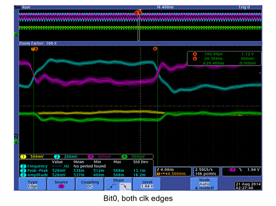
    Also when CLKOUTP/CLKOUTN cross on my scope, data is not center aligned.

    1. Red signal is CLKOUTP, Blue is CLKOUTN, Green is bit0, Yellow is bit1
    2. 1st clock edge (falling) captures bit0 as a ‘1’, for a value of 3F?
    3. 2nd clock edge (rising) captures bit0 as a ‘0’, for a value of 3E.
    4. This doesn’t match page 58 of adc58c48 data sheet!

    Thanks,

    Todd Moore

    University of Illinois

  • Todd,

    Thanks for sharing the scope plots. I agree that the timing diagrams are a bit misleading but they are not drawn to scale. Referencing the setup time for the DDR LVDS interface on pg 8 of datasheet, tsu is between 500ps to 1.1ns so 0x3E comes out first before 0x3F. This resembles more of an edge aligned interface and you will need to delay the clock to properly latch the data.

    Thanks,

    Eben.

  • Eben,

    Thanks again for clarifying the datasheet!  The scope plot above is taken from a TI ADS58C48EVM connected to a TI TSW1200EVM.  I've attached the probes (thru wires soldered onto CHB<0>_P, & CHB<2>_P signals) directly to the output of the adc.  The CLKOUTP signal is being driven by the adc.  I expected the clock signal to be aligned better with the data. So the TSW1200EVM must be delaying CLKOUTP/N in order to capture the correct signal.  I'll provide some delay in my design to account for the clock signal.

    Thanks again for the clarification,

    Todd Moore

    University of Illinois