This thread has been locked.

If you have a related question, please click the "Ask a related question" button in the top right corner. The newly created question will be automatically linked to this question.

ADS42LB69 Serial Interface Timing

Other Parts Discussed in Thread: ADS42LB69

Dear Sir,

I have a couple of questions about the ADS42LB69 serial interface timing those I could mot find specific data in the data sheet. I am referring page 44 and 45 in the datasheet.

1)  I would like to know minimum time to hold SEN high after SEN low to high. In other word how soon SEN can be set to low (active) after SEN was set to high (disable) as a minimum interval time for register access.

2) What is maximum delay time (set up time) from SCLK to SDOUT at Serial Register Readout?

Best regards,

Masa

  • Hi Masa,

    1) Minimum duration for a pulse on SEN is 25ns

    2) The maximum delay time is the same as the minimum setup time and this is also 25ns.

    Thanks,

    Eben.

  • Hi Eben,

    Thank you very much for the answer.

    Masa

  • Hi Eben,

    I have another 3 questions.

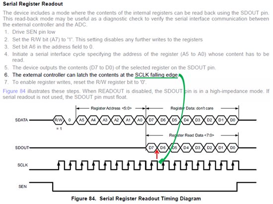
    1) On page 45 in the datasheet, it explains as follows; 

        "6.  The external controller can latch the contents at the SCLK falling edge."

        However Figure 84 looks SCLK rising edge. Which is correct?

        SDATA for address looks rising edge even at Readout? SDOUT and SDATA are not same timing?

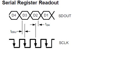
    2) I would like to make sure (again) what are  

         Max tDH(SCLK latch to max SDOUT hold time), and

         Min tDSU (min SDOUT time to SCLK latch).


    (Above assumed SCLK falling edge instead of rising edge for latching SDOUT.) 

     3) Min fSCLK is spcified as "> dc" in the table 8 on page 44 in DS. Does it means SCLK can NOT be stopped? 

       In another quesion, I asked what is behavior at SCKLK is stopped without xpecting getting into Sandby mode.

    Best regards,

    Masa  

  • I inserted the timing block diagram (SDOUT vs. SCLK timing) for question #2 in my previous solt.

  • Hi Eben again,

    Sorry for sending many. I would ike to correct #3 question, that I did not ask you yet. I asked CLK(CLKINP/CLKINN) not SCLK. So I would like to undertand if SCLK should NOT (can NOT) be stopped.

    And timing between SCLK and SDOUT, I am asking for securing to latch data from ADC as desig nmargin with FPGA, so if you have a distribution data of SDOUT timing. It will be very helpful.

    Best regards,

    Masa 

  • Eben,

    May I get answer?

  • Hi Masa,


    Q1)  The SPI interface of ADS42LB69 uses the rising edge of SCLK to latch data and address. For maximum setup and hold times for a given clock period, we recommend that the external controller uses the falling edge of SCLK to send data and address to the SPI interface of ADS42LB69. 

    Q2)There is no spec for max(tDH) since it is dependent on the period of SCLK that is being used. Min tDH and Min TDSu are both 25ns.

    3)Min fsCLK>dc means to be able to read and write to the SPI interface, you need to provide a clock at SCLK. If you are not reading or writing to the SPI, then SCLK can be stopped.


    Thanks,

    Eben.

  • Hi Eben,

    Thank you very much for your response. I understand that ADS42LB69 data ltach timing using SCLK rising edge, and falling edge is recommneded to use for external controller.

    I would like to make sure if my understand is correct using the follwoing figure (Figure 84 on page 45 in ADS42LB69 datasheet)


    ADS42LB69 latched SDOUT(D7) at SCLK rising edge.  Then it is recommended that external controller readout SDOUT(D7) at SCLK falling edge. I marked green and red arrows on the Figure 84. 

    Is my understanding correct?

    I think that the Figure 84 needs to be corrected SDOUT location shiftted to right a little (open D7 eye  at SCLK rising edge) and SDOUT(D7) will hold data until SCLK falling edge (red arrow). Like below. Is this correct? 


    Best regards,

    Masa

  • Hi Masa,

    Yes, your understanding is correct. The ADS42LBx9 latches the data on the rising edge so we recommend the external controller to use the falling edge to launch the data

    The timing diagrams are not drawn to scale and are only meant to show the order of the address and data. All relevant timing information such as setup and hold times are given in Table 4 on page 35.

    Thanks,

    Eben.

  • Eben,

    I assume that you possibly refer ADS42JBx9 Datasheet since Table 4 on page 35 which is you pointed is the timing for Table 8 on page 44 of ADS42LBx9 Datasheet.

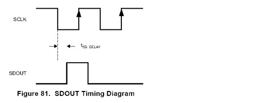
    I found that the ADS42JBx9 Datasheet describe below on page 36. (ADS42LBx9 does not have this).

    This will make clear timing relationship betwwen SDOUT and SCLK.

    However I found that ADS42JBx9 Datasheet describes "The external controloler can latch the contents at the SCLK rising edge."  on page 35.

    ADS42LBx9 Datasheet describes  "The external controloler can latch the contents at the SCLK falling falling edge." on page 45.

    Please let me make sure if both devices are different in SDOUT/SCLK behavior. I need timing relationship between SDOUT and SCLK for ADS42LB69.

    Best regards,

    Masa 

  • Hi Masa,

    Thanks for pointing out the differences. I have confirmed that during SPI Read, data on SDOUT should be latched on the rising edge by the external controller for both ADS42JBx9 and ADS42LBx9. The ADS42LBx9 datasheet will be corrected accordingly.

    During SPI Write, the external controller has to launch the data on SDATA on the falling edge so that it can be latched on the rising edge by ADS42LBx9

    Thanks,

    Eben.

  • Hi Eben,

    Thank you for your correction.

    May I have Max and Min of tSD_DELAY in Figure 81 on page 36 in ADS42JBx9?

    20ns sounds tyical. SDOUND will be read at rising edge but I would like to know the Max/Min from falling edge. 

    Best regards,

    Masa

  • Eben,

    May I have your answer?

    Masa

  • Hi Masa,

    We guarantee that data will be available on SDOUT before the rising edge of SCLK if the period of SCLK is less or equal to 50ns. Please treat tsd_delay of 20ns as the worst case or maximum delay for data to be available on SDOUT relative to SCLK falling edge. There is no minimum tsd_delay defined for the SDOUT/SCLK interface. 

    Thanks,

    Eben.

  • Eben,

    Thank you very much.

    Masa