This thread has been locked.

If you have a related question, please click the "Ask a related question" button in the top right corner. The newly created question will be automatically linked to this question.

ADS5282 - Can't sample low frequency signals

Expert 2370 points
Other Parts Discussed in Thread: ADS5282, THS4509

Hi,

I am using ADS5282 EVM interfaced with FPGA via HSMC bridge.

My goal is to sample 50 Hz signal with some 1 MHz frequency but minimum clock which can be used with ADS5282 is 10 MHz. I don't mind using even 10 MHz clock but it doesn't sample signals properly below 50 kHz.

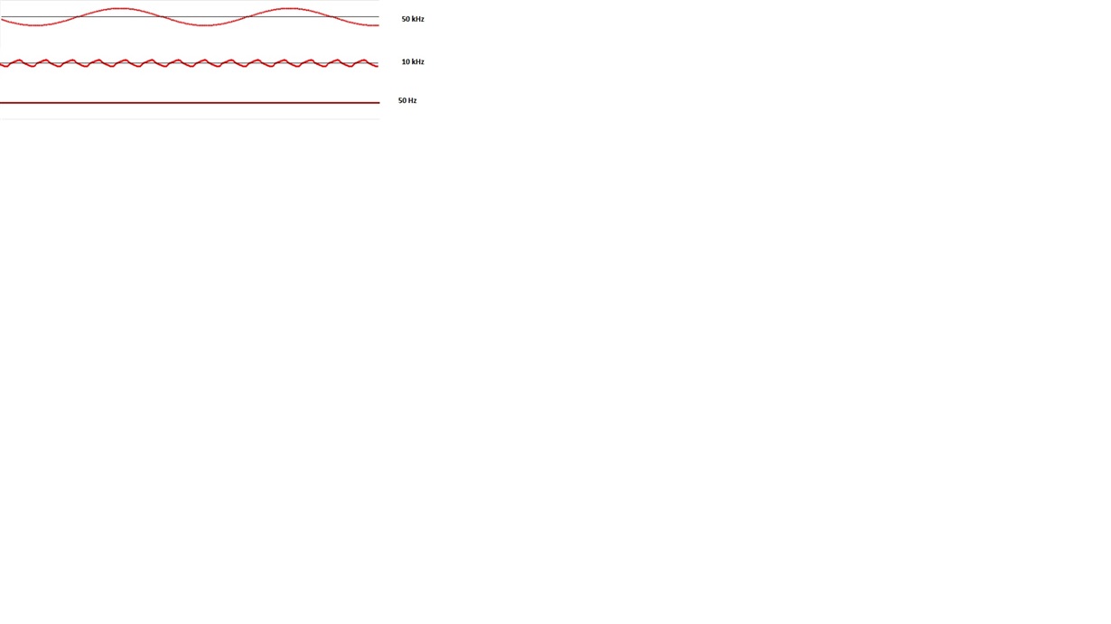
I am attaching snapshots of the signals with 50 kHz, 10 kHz and 50 Hz, respectively sampled with 10 MHz clock.

You can see 50 kHz signal is sampled properly but 10 kHz and 50 Hz signals are not sampled correctly. Although the sampling clock is too much it doesn't show much samples in case of 10 kHz and 50 Hz signals.

Can you tell what is wrong ? How to sample low frequency signals properly ?

Thanks.

BAS

  • Hi,

    Take a look at the schematics for the EVM that are included in the User Guide.  You will see that the input path of the EVM uses a transformer to convert a single ended input to balanced differential for the ADC, and that the AC coupling of the transformer allows the signal to be biased to the desired voltage levels for the ADC.    Google the TC1-1t transformer and you can see that the 3dB bandwidth of the transformer is 400KHz on the low side.  Lower frequencies can pass through but with more attenuation.  50Hz is way too low to get through the transformer.

    If you want to input a frequency that low you will need to do your signal conditioning external to the EVM and that would include making the signal balanced differential and biased to the desired voltage (the VCM voltage of the ADC.  The on the EVM itself you would have to install the optional second SMA for the normally unused other leg of the differential path and remove the transfomers and shunt across their pads with zero ohm resistors.  Usually for low frequency input the input circuit needs to be an amplifier device, DC coupled, fully differenital output, with a VCM input pin of the amp that can be used to biias the output levels to the desired VCM.   Some of our older EVMs might include a THS4509 amplifier on one channel that can be used for a DC coupled amplifer input path with some soldering, but that was not done on this EVM.

    Regards,

    Richard P.

  • Hi Richard,

    Thanks a lot.

    Is there any way to use sampling clock lower than 10 MHz ?
  • Hi,

    No, 10Msps is the datasheet minimum for the sampling clock.  Since this device serializes the sample data out onto a single LVDS pair per channel, there must be a PLL in the ADC to create the higher speed bit clock for the serialization and to be able to output the LVDS LCLK to go with the serialized data.  The PLL itself will have a min to max range of operation over frequency and 10MHz is what we guarantee on the low side.

    Regards,

    Richard P.

  • Hi,

    Thanks Richard.

    What reference voltage should be used to normalize the sampled data ?

    That's how I am doing this,

    (Output / 4096) - Vref

    Thanks.

  • Hi,

    I don't know what you want to do with the sampled data or what you mean by normalize in this context.  The output sample codes correspond to a differential input signal, so that the code 0000 0000 0000 represents -1.00V differential input while a 1111 1111 1111 code represents +1.000V differential input. (offset binary representation)    VCM does not affect that relationship, within the allowable range of VCM which may be +/- 50mV to +/-200mV depending on the particular data converter being used.  If 2.00V is full scale, then each lsb of the code represents 2.000V / 4096 = ~488mV. 


    Regards,

    Richard P.

  • Hi,

    I want to convert the sampled data into actual signal amplitude which is 1 Vpp in my case. 

    Usually reference voltage is compared against the input signal to give digital output which tells us what fraction of the reference voltage or current is the input voltage or current. Therefore, I asked about the reference voltage.

    By 2 V full scale, do you mean amplitude of the input signal or the reference voltage ? If that's amplitude of the input signal then it doesn't sample properly in my case. It samples sine wave properly as long as the input signal is 1 Vpp. 

    If you see ADS5282 datasheet, Pg no. 3, RECOMMENDED OPERATING CONDITIONS, Differential input voltage range is 2 Vpp and Clock setting is 3 Vpp but it doesn't sample properly with signal amplitude 2 Vpp as I told earlier. It does work with 1 Vpp. I am bit confused about the settings. Can you tell what should be the maximum clock and input signal amplitude ? 

    There is also Analog supply voltage (AVDD) which is 3.3V, I wonder if that will be used to convert the output to actual signal amplitude ?

    One more thing I just noticed that it doesn't sample 1 MHz sine wave properly with Fs = 40 MHz. Maximum sampling frequency is 65 MSPS, do I need to do something to achieve 65 MSPS sampling frequency ?

    Thanks for your help.

    -BAS

  • Hi Richard,

    I appreciate your quick help.

    Thanks.

    -BAS
  • Hi,

    The default full scale input voltage definition is 2.00V peak to peak differential.  Differential means that each side of the diff pair has a peak to peak swing of 1.000V.   So if both sides of the input signal is biased up to a common mode level of 1.5V, then the IN+ signal will swing between 1.0V to 2.0V.  (That is a 1V peak to peak swing around the VCM voltage.)  And at the same time the IN- signal will swing between 2.0V and 1.0V.  (Which is a 1V peak to peak swing around the VCM level.)  But since the IN+ and IN- are opposite each other, while in+ is at 1V and IN- is at 2V, the differential input voltage is -1.0V which corresponds to the negative side of the full scale range. And while IN+ is at 2V while IN- is at 1V, then the differential input voltage is +1V which is at the positive end of the full scale range.  So the peak to peak *differential* input voltage is 2V peak to peak differential.  But each side of the dif pair only swings between +/- 0.5V around VCM.    and VCM does not play into the determination of what the output codes are.  Since the differential input signal is to be symmetrical and balance about VCM at all times, VCM only describes the absoute level about which the differntial signal is biased -but does not affect what the differential input voltage *is*.  For example, if IM+ is at 1.75V, then IN- must be at 1.25V at that moment for a diffential input of 0.5V which would correspond to an output sample code of about 1100 0000 0000 or about 3/4 the way to positive full scale.

    I go through all this because i suspect what we call 2V peak to peak differential might correspond to what you call 1V.

    Operating the ADC at 40 MHz sample rate would be fine.  You don't have to operate at 65MHz sample rate.  But if you are using our EVM or using some kind of transformer coupling in your design, make sure the 1MHz analog input signal is within the bandwidth of the transformer coupling.  The ADC itself doesn't care if the input tone is 1MHz or something else.   Having a clock swing of 3V peak to peak would be plenty big enough.   but pay attention to the input clock requirements on page 35.  The clock may be differential or single ended, but the appropriate bit in the SPI register space must be set for single ended or differential as needed.  I believe the default power up value for this bit is for single ended clock while our EVM is set up for differential clock, so we always have to use the SPI GUI to set this bit for differential clock.

    So VCM in this case is not the same as the reference voltage you speak of.   If the actual sampling front end were single ended then i suppose the reference voltage used for the conversion would be 2V if full scale were 2V.  But the sampling front end in this case is differential.  And you can see on pg 5 of the data sheet that VREFtop is 2.5V while VREFbottom is 0.5V.  That is 2V, and is centered about 1.5V VCM.   In Internal reference mode, the device drives VREFtop and VREFbottom to these voltages with some tolerance.  In external refernece mode, you must supply these voltages to these pins.   (External reference is usually used where someone wants to use many devices and wants to remove the device-to-device mismatch in full scale between devcies and give all the devices the same references to tighter tolerances than internal reference supplies.

    So your input circuit to couple your signal to our ADC must do some signal conditioning to make your max signal match up to our full scale definition, as well as biasing up the differtial signal to our required VCM voltage.   Whatever you have to do to condition your signal to the data converter input requirements will determine how you have to relate the output sample codes back to your input signal levels.

    Regards,

    Richard P.